Introduction
The chemical and physical properties of most material can be altered by the addition of impurities or dopants [1].
Doping can be achieved by different technology techniques. Diffusion is still one of acceptable and important methods in such a field. Doping has many important technological applications [2,3]. For example, doping makes it possible to prepare alloys which possess low surface energy in the metallic surface, which is the condition to realize drop wise condensation on such surfaces. This in turn has important technological applications.
Moreover, addition of specific dopants in small percentages in semiconductor, such as silicon, controls electronic conduction processes and forms the basis of solid state device technology, such as the fabrication of the integrated circuits (IC)[4].
The temperature dependence of the activation energy and diffusion coefficient “D” of Born “B” and Phosphorus “P” in silicon suggest that such diffusion is mediated predominantly by interstitials.
In general, diffusion is the physical phenomenon where materials (atoms) move from high concentration regions to low concentration regions driven by thermal motion of particles[5] . Diffusion occurs with a rate proportional to the concentration gradient between the two regions [6].The maximum concentration of dopant that can be dissolved under equilibrium condition without forming a separate phase is termed as solid solubility [7].
Dopants in diffusion mechanism are deposited on the substrate surface and driven-in by high temperature annealing.
Ion implantation is by contrast a non-equilibrium process, the dopant atoms being driven into the solid by violent use of their excess kinetic energy. Even in ion implantation some ions will not penetrate the target surface but will be reflected by collision with outer most layers of atoms.
In diffusion mechanism, an atom must surmount the potential energy barrier presented by its neighbors.
In practice, the diffusion process is suggested to consist of two steps. At the first step the wafer is exposed to impurity source for the entire duration of the diffusion [8]. As a result the dopant is deposited on the wafer surface to form a high surface concentration.
The second step is called drive – in diffusion, in which, the slices are next heated (100oc-1200oc) in O2 or N2 atmosphere and the dopant diffuses or (driven –in) into the target slice.
A mass transfer model for doping a metal target at elevated temperatures has been built up9 based on transport of ions in matter and radiation enhanced diffusion. The process was simulated by a dynamic Monte Carlo (MC) method [9]. The diffusion equations for the implanted species and vacancies with moving boundaries are considered to calculate concentration-depth profiles.
A single step diffusion model is considered [10]. Early in the development of integrated circuit fabrication technology, semiconductor doping was accomplished by exposing semiconductor substrates to high concentrations of the desired impurity, exceeding the level required to achieve solid solubility of the dopant at the semiconductor surface.
The atomic diffusion has been calculated by many other authors [11-13].
The development of theoretical calculation of atomic diffusion is still of great interest.
The aim of the present trial is to solve the parabolic diffusion equation using Fourier’s series expansion technique. This makes it possible to obtain the concentration function and the doping penetration depth within the substrate target.
Doping of indium, phosphorus, gallium and Arsenic into Silicon as an illustrative examples are considered.
Mathematical Formulation of the Problem
There are different mechanisms of atomic diffusion (substitutional), vacancy, interstitial or combination mechanism known as interstitially mechanism) [14].
As a result an initially localized substance of one species (impurity dopants atoms) will be redistributed throughout a background medium (target) due to the gradient of concentration and due to random thermal motion.
High temperature processing will be considered.
In setting up the problem, one will consider a target Silicon slab subjected to a flux (J0 m-2s-1) of impurity atoms of one species (indium, phosphorus, gallium or Arsenic) moving along the x-axis perpendicular to the front surface of the target.
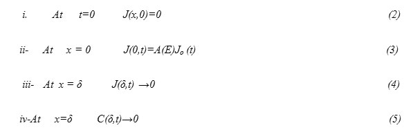
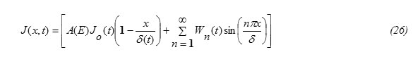
It is also suggested that the impurity atoms are supplied from an undiminished, infinite source for the entire duration of the diffusion process as in [8]. At the front interface some of the impurity atoms will be reflected, whereas a part A(E) J0(t) will be driven-in the target slab. Where A(E) stands for an equivalent absorption coefficient which depends in general on the energy (E) of the impinging impurity atoms and may be a function of the surface temperature. This driven in part will be redistributed within the target wafer till a penetration depth δ(t) at which the concentration of the impurity atoms equal or nearly equal to zero (or even equal to the background concentration) .
In analogy to heat transfer, one can combine Fick’s first law and the continuity equation together with the heat diffusion equation to write the mathematical formulation of the problem. The diffusion equation is written in terms of the flux J(x,t) density rather than the concentration C(x,t) m-3 of the impurity atoms as follows:
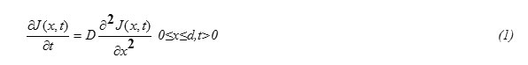
Where D (m2/s) is the diffusion coefficient of the target material.
Equation (1) is subjected to the following conditions
To solve equation (1) it is transformed into a nonhomogeneous equation subjected to homogeneous conditions encountered on the space variable x [15]. This can be fulfilled as follows:
Assuming that the required solution can be written in the form
J(x,t) = V (x,t) + W (x,t) (6)
Inserting equation (6) into equation (1) one gets
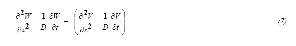
With boundary conditions
W(0,t)=A(E)Jo(t)-V(0,t) (8)
W(δ,t)=-V(δ,t) (9)
The function V(x,t) has to be chosen so that the boundary conditions (8) and (9) become homogeneous.
To meet such requirements, let us choose
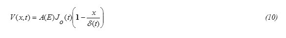
This makes it possible to write the following homogeneous conditions
W(x,0)=0 (11)
W(0,t)=0 (12)
W(δ,t)=0 (13)
Substituting equation (10) into equation (7) one gets the equation for W(x,t) in the form
formula14
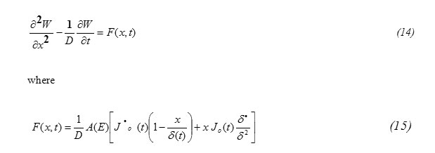
To solve the inhomogeneous equation (14), let us use the Fourier series expansion Technique , according to which, let us assume the solution to be in the form:
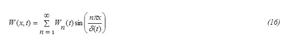
which satisfies the conditions (12) and (13).
The condition (11) implies that
Wn(0)=0 (17)
Also one suggests the function F(x,t) to be in the form
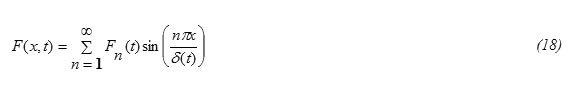
Substituting equation (16) and (18) into equation (14) one gets
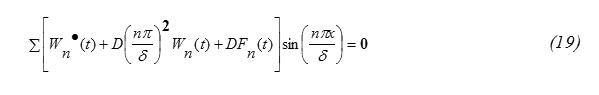
Since sin(nπx/δ) ≠0 in equation (19) one gets
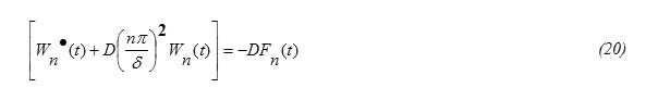
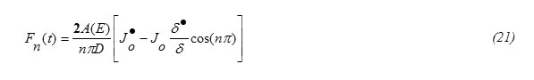
Applying the orthornormality property on Fourier series one gets from equations (15) and (18), the expression for Fn(t) in the form
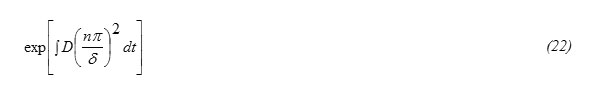
Equation (20) has an integrating factor as following
and thus the solution can be obtained in the form
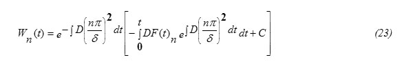
The condition at t=0, Wn(0)=0 gives C=0 , thus
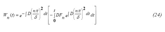
Hence, one can write the expression for W(x,t) in the form
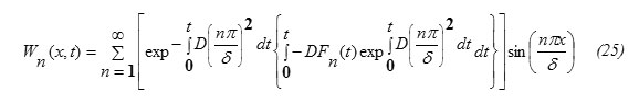
From equations (6) and (25), the solution of equation (1) is obtained in the form
Determination of the Concentration Function C(x,t)
This can be fulfilled as follows:
i) From Fick’s first law
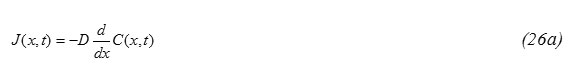
Thus
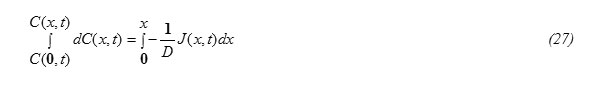
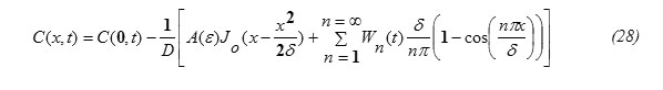
Substituting the expression for J(x,t) , eq.(26) into eq.(27) and performing the required integrations , one can get the following result:
ii) To find the expression for C(0,t), let us apply the balance equation for the particle flux, written in the form:
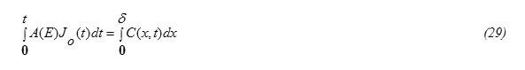
this gives
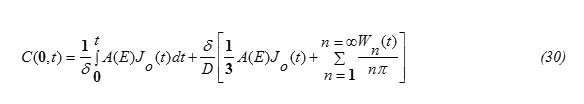
Substituting equation (30) into equation (28) one gets the concentration function in the form:
Determination of the Diffusion Penetration Depth “δ”
This can be obtained from the condition (5). Substituting x=δ in equation (31), one gets
Computations
The concentration function C(x,t) (m-3) (eq. 31) for the special case when the incident particle flux J0 is constant and A(E)=1-R(T), for diffusion of indium, phosphorus, gallium and Arsenic in Silicon target are computed. For the special case J0 is constant as an illustrative example. For such a case Fn(t)=0 , Wn(t)=0 and
This result eq.(33) is in analogy to the expressions for δ published in some literatures [5,15]. Eq.(32) shows also that the diffusion depth is determined mainly through the diffusion coefficient D for the target material. Wn(t) can be obtained by substituting from equations 21,33 into equation 25. It worth to note that [16] ,
D = D0 Exp (- Ev | kT). (34)
Where D0 is the temperature independent diffusion coefficient and Ev is the activation energy. The parameters for each case are given in Tables (1,2).
![Table 1: The values of D0 , Ev for the diffused elements of Phosphorus, Gallium , Indium and Arsenic diffused into Silicon target material [14].](http://www.materialsciencejournal.org/wp-content/uploads/2014/12/Vol11_No2_Diffus_M.K_T1-150x150.jpg) |
Table1: The values of D0 , Ev for the diffused elements of Phosphorus, Gallium , Indium and Arsenic diffused into Silicon target material [14].
Click here to View table
|
Table 2: Size of some impurity atoms relative to Silicon [16].
|
Element
|
Size relative to silicon
|
|
Gallium
|
1.07
|
|
Indium
|
1.22
|
The concentrations C(x,t) (m-3) are illustrative graphically in figures (1-8), when the diffusion of indium, phosphorus, gallium or Arsenic into Silicon are obtained as a function of diffusion time and diffusion depth respectively.
Computations
Computations are carried out according to values in Table 1 [14] , considering constant incident particle flux J0 = 5´1015 m-2 sec-1 and R(T) for silicon = .322+ 3.12 x 10⁻⁵T in the range (300 K – 1685 K) [15].
It is suggested that the relative size of the dopant atom relative to the host medium atoms plays also an important role in the diffusion process. Table 2 , gives the size of the impurity Gallium and Indium atoms relative to Silicon [16].
Table 3, gives the electron configuration of neutral atoms in their ground states is related also to the size of the diffused atoms.
Table 3: The outer configuration for some neutral atoms in their ground states .
|
Element
|
Electron configuration
|
|
Si14
|
3s23p2
|
|
P15
|
3s23p3
|
|
Ga31
|
4s24p
|
|
As33
|
4s24p3
|
|
In49
|
5s25p1
|
The following special cases are considered:
i) t = 1 sec.
The concentration function C(x,t) against the depth “x” is computed for the diffusion of Indium, Phosphorous, into Silicon (Figure 1, R = 3.313 E-1 for T = 300 K, and Figure 2, for R = 3.5 E-1 and T = 900 K).The same dependence for the diffusion of Arsenic and Gallium, into Silicon (Figure 3, for R = 3.313 E-1 and T = 300 K, Figure 4, for R = 3.5 E-1 and T = 900 K).
ii) At x = ( δ /10) m
The concentration function C(x,t) against the diffusion time t is computed for the diffusion of Indium, Phosphorous, into Silicon (Figure 5, for R = 3.313 E-1 , T = 300 K and Figure 6, for R = 3.5 E-1 , T = 900 K). The same dependence for the diffusion of Arsenic and Gallium, into Silicon (Figure 7, for R = 3.313 E-1 and T = 300 K, Figure 8, for R = 3.5 E-1 and T = 900 K).
Discussions
1-The obtained expression for the concentration function C(x,t) m-3 (equation 31) reveals that it depends principally on the flux density J0 m-2s-1. The dependence is linear for constant flux density.
2-The same function depends fundamentally on the diffusion coefficient D , m2s-1 .
3-Dopants of higher relative sizes are more accumulated than dopants of smaller relative sizes at a certain layer and at a certain diffusion time (Figures 1, 2, 3 and 4).
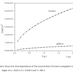 |
Figure1: Shows the time dependence of the concentration of Arsenic and gallium in silicon target. At x = δ/10 m, R = 3.313E-1 and T = 300 K
Click here to View figure
|
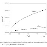 |
Figure2: Shows the time dependence of the concentration of Arsenic and gallium in silicon. At x = δ/10 m, R = 3.3501E-1 and T = 900 K
Click here to View figure
|
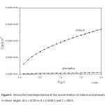 |
Figure3: Shows the time dependence of the concentration of indium and phosphorus in silicon target. At x = δ/10 m, R = 3.313E-1 and T = 300 K
Click here to View figure
|
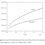 |
Figure4: Shows the time dependence of the concentration of indium and phosphorus in silicon target. At x = δ/10 m, R = 3.3501E-1 and T = 900 K
Click here to View figure
|
4-The diffusion penetration depth depends basically on the diffusion coefficient D m2s-1 which in turn depends on the absolute temperature T. So the penetration depth becomes greater and the concentration becomes smaller at T = 900 K than that at T = 300 K. Such depth depends also on the size of the dopant atom relative to the host atom, this is evident in figures: 5, 6, 7 and 8.
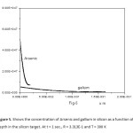 |
Figure5: Shows the concentration of Arsenic and gallium in silicon as a function of the depth in the silicon target. At t = 1 sec., R = 3.313 E-1 and T = 300 K
Click here to View figure
|
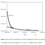 |
Figure6: Shows the concentration of Arsenic and gallium in silicon as a function of the depth in the silicon target. At t = 1 sec., R = 3.3501 E-1 and T = 900 K
Click here to View figure
|
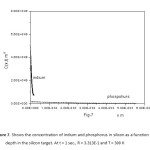 |
Figure7: Shows the concentration of indium and phosphorus in silicon as a function of the depth in the silicon target. At t = 1 sec., R = 3.313E-1 and T = 300 K
Click here to View figure
|
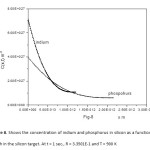 |
Figure8: Shows the concentration of indium and phosphorus in silicon as a function of the depth in the silicon target. At t = 1 sec., R = 3.3501 E-1 and T = 900 K
Click here to View figure
|
Conclusions
- The concentration of the Indium and Arsenic dopants into Silicon at a certain layer with time is greater than that for Phosphorous and Gallium dopants into Silicon for the same operating conditions.
- The penetration depth of the Indium and Arsenic are less than the Phosphorous and Gallium into Silicon for the same operating conditions.
References
- Carter G, Grant W A , Ion Implantation of Semiconductors, Edward Arnold, London, (1976).
- Kemarov F, Ion Beam Modification of Metals, Gordon and Beach Science Publisher, Tokyo (1992).
- Zhao Q, Zhang D C & Lin J F, Int J. Heat Mass Transfer ,34 No.11, (1991) 2833.
CrossRef
- Hung V, Hong P& Khue B, Prac. Nalt. Cenf, Theor. Phys, 35 (2010) 73.
- Narayanan M, Al-Nashash H, computer and electrical engineering, doi:10.1016, (2008).
- Kittel C, Introduction to solid state physics ( John-Wiley & Sons),1997, Ch.17;p.542.
- Gary S M, Simon M S, Fundamental of semiconductor fabrication, 1st ed. (John- Wiley and Sons Int.), 2004.
- Morgan D V, Board K, An introduction to semiconductor micro technology, 2nd ed.( Jon-Wiley & Sons) , 1990.
- Chang H W , Lei M K, computational material science, 33, (2005) p.459.
- Jones S W, Diffusion in Silicon, (IC Knowledge LIC),2000.
- Xie J, Chen S P, J. Phys. D, 1252 (1999).
- Anna J, Colombo L & Nieminen R, Phys. Rev. B 64 (2001) , 233203.
CrossRef
- Chroneos A, Bracht H, Grimes R W & Uberuaga B P, Appl. Phys. Lett., (2008) 172103.
CrossRef
- Tsang W T , Schubert E F, Sugino O, & Oshiyama A, phys. Rev. B, 46 (1992) , 12335.
- Eckert E R G, Drake R M, Analysis of heat and mass transfer (Int.Student Edition, McGraw-Hill , Tokyo ),1972.
- Nchols C S, Van de Walle C G & Pantelides S T, Phys.Rev. B, 40 (1989), p.5484.
CrossRef
- Stephenson G, An introduction to partial differential equation for science student(Longmans, UK) ,1968, Ch.4.
- Dwight H B, Tables of Integrals and other mathematical date, 4th ed. (Macmillan company, New York), (1961) , p.84.

This work is licensed under a Creative Commons Attribution 4.0 International License.

