
Structural, Optical and DFT Analysis of Pure and Cd doped PbS Thin Films Deposited by Chemical Route
 , Neha Prashant Chaware2, Karankumar Ramnath Sature3, Sajid Naeem4, , Umesh Jagannath Tupe6, Nanasaheb Pandharianth Huse2and Arun Vitthal Patil1, , *
 1Department of Physics and Research Center, MGV’s MSG Arts, Science and Commerce College, Affiliated to Savitribai Phule Pune University, District Nashik, Malegaon, India
2Advanced Materials and Interfaces Lab, Department of Physics, G. T. Patil Arts, Commerce and Science College, Affiliated to Kavayitri Bahinabai Chaudhari North Maharashtra University, Nandurbar, India
3Department of Physics, J.E.S., R. G. Bagdia Arts, S. B. Lakhotia Commerce and R. Bezonji Science College, Affiliated to Dr. Babasaheb Ambedkar Marathwada University, Jalna, India,
4Department of Applied Sciences, Maulana Mukhtar Ahmad Nadvi Technical Campus, Affiliated to Savitribai Phule Pune University, Malegaon, India
5P.G. Department of Zoology G. T. Patil Arts, Commerce and Science College, Affiliated to Kavayitri Bahinabai Chaudhari North Maharashtra University, Nandurbar, India
6Department of Electronic Science, Vidya-Amrut Dnyan Pratishthan's Arts, Science and Commerce College, Shirsondi, Tal- Malegaon, Dist: Nashik Affiliated to Savitribai Phule Pune University, India
7Department of Physics, MGV’s, Arts, Science and Commerce College, Affiliated to Savitribai Phule Pune University, Nimgaon, Tal-Malegaon, India
Corresponding Author E-mail: aruptl@gmail.com
Download this article as:
ABSTRACT:Herein, we report successful deposition of undoped and cadmium-doped lead sulfide thin films onto silica glass substrates employing the chemical route. XRD analysis confirmed the formation of a cubic rock-salt structure (with (111), (200), and (220) reflections) for all prepared samples. A marginal displacement of the diffraction peaks towards elevated 2θ values was observed after Cd doping, indicating lattice contraction due to the substitution of Pb²⁺ (1.19 Å) by smaller Cd²⁺ ions (0.97 Å). Williamson–Hall analysis showed the crystallite size decreased from 13.66 nm (pure PbS) to 13.45 nm at 10% Cd doping, accompanied by a rise in microstrain from 1.69 × 10⁻³ to 5.88 × 10⁻³, before increasing to 16.32 nm at 20% Cd doping as the strain relaxed. UV–Vis. spectroscopy revealed enhancement in optical bandgap of 1.6 eV for pure to 2.2 eV and 2.4 eV for Cd-doped PbS thin films (10% and 20%), respectively, demonstrating that Cd doping effectively tunes PbS from a narrow-gap infrared absorber toward gap values more suited to visible-light photovoltaic harvesting. FESEM analysis revealed a uniform, compact surface morphology with doping-dependent grain evolution. EDX analysis confirmed the successful deposition of Cd into the PbS lattice with no detectable impurity phases. Density functional theory calculations executed using Quantum ESPRESSO supported the experimental observations and revealed significant changes in the electronic band structure due to Cd incorporation, with the computed bandgap increasing from 0.46 eV for pure PbS to ~2.0 eV upon Cd substitution (HOMO/LUMO at 7.85/8.21 eV), confirming a direct reconstruction of the band edges rather than mere defect-state formation. The results of this study reveal that incorporating cadmium (Cd) into PbS lattice successfully fine-tunes their properties, which in turn improves their promise for use in photovoltaic applications.
KEYWORDS:Cd incorporation; Chemical bath synthesis; Electronic band structure; Energy band gap; PbS nanostructured thin films
Introduction
Lead sulfide possesses remarkable physical properties, such as a tunable band gap, that set it apart from many other semiconductors. The hardness of Lead sulfide (PbS) is very high, and its material strength also contributes greatly to its strong properties.1 In recent years, PbS has found widespread utility across a diverse range of optoelectronic and solar cell applications, including photodetectors, infrared sensors, photoresistors, solar absorber layers, solar control coatings, and thin-film photovoltaic devices.2 PbS belongs to IV-VI group semiconductor and has direct bandgap of nearly 0.41 eV at ambient temperature. Its unique properties, including a narrow bandgap, large excitonic Bohr radius (~18 nm), and strong optical absorption coefficient (~10⁵ cm⁻¹), make it highly attractive for optoelectronic and photovoltaic applications. PbS has a wavelength in the far-infrared part of the electromagnetic spectrum because of its very small band gap of only 0.41 eV at room temperature.3 Cadmium was selected as the dopant owing to its similar ionic radius to Pb²⁺, which enables substitutional incorporation into the PbS lattice without inducing significant structural distortion, while simultaneously widening the bandgap and improving band alignment with CdS, a well-established window layer material factors that collectively enhance the suitability of Cd-doped PbS for photovoltaic applications.2,4
Lead chalcogenides, including PbS, are among the most researched materials for infrared (IR) luminescence due to their distinctive properties, including large dielectric constants, ferroelectric effects, large Bohr radii, and direct band-gap transitions Also, because the electron and hole effective masses are small and nearly equal, PbS is a good material for infrared detectors and other optoelectronic devices.3,5 One of the most remarkable properties of PbS is the strong quantum confinement caused by its large exciton Bohr radius of 18 nm, which is an important feature for quantum dot-based devices, enhancing their performance in IR imaging, light harvesting, and other applications.6 PbS already finds broad applications in the field of photography, as Pb²⁺ ion-selective sensors, optical switches, solar absorbers, and many more.7 Its prospects for application in optoelectronic devices also continue to make it a highly valuable material.8
Several deposition factors in chemical bath deposition method, including precursor content, temperature, and cadmium doping, have been studied with respect to the optical and structural properties of undoped and Cd doped PbS thin films.9 The effects of precursor concentration on the size and uniformity of PbS grains were also investigated, and the results showed that the optimized films exhibit improved charge-transport properties, which are essential for efficient devices.10 Cadmium doping has also been reported to enhance the crystallinity and electrical properties of PbS thin films. In chemically deposited nanostructured PbS, Cd incorporation typically widens the optical bandgap through a combination of quantum confinement and lattice alloying effects, while simultaneously modulating carrier transport behaviour.11 Furthermore, PbS/CdS heterostructures have been fabricated and shown to yield promising photodetection performance across both the UV and near-infrared regions, underscoring the potential of such heterojunctions for broadband, multi-spectral optoelectronic devices.12 Chemical bath deposition (CBD) stands out as a comparatively simple and economical method. It presents several advantages over other deposition techniques, particularly its scalability for large-area/large-scale production and the durability of the deposited films, rendering it a favourable choice for commercial applications.13,14 However, despite the previous research on the structural, optical, and electrical properties of Cd-doped PbS thin films, the correlation between the experimentally observed properties and the theoretically predicted electronic structure is not yet fully established. Particularly the combination of the properties of pure and Cd-doped PbS thin films prepared by the chemical route with the help of structural and optical characterizations and first principles Density Functional Theory calculations provide some additional insight into the Cd incorporation mechanism and its impact on the electronic structure and optical properties of PbS. For this reason, the current research explores the preparation of pure and Cd-doped PbS thin films by the chemical route. The study also involves the structural and optical characterizations of the produced thin films and applies the Density Functional Theory calculations to investigate the modification of the electronic structure and band-gap properties of PbS caused by Cd doping. The obtained results and their analysis contribute to the understanding of Cd’s influence on PbS and its potential application in optoelectronics and photovoltaics.15
Materials and Methods
Thin-film technique
Pure and cadmium Cd doped PbS thin films were grown on precleaned silica glass substrates using the chemical bath deposition method. Before deposition, the glass substrates underwent ultrasonic cleaning in a chromic acid solution, laboratory detergent, and deionized (DI) water, then dried. Lead nitrate (0.06 M) served as the Pb precursor whereas cadmium sulfate served as the dopant source at concentrations of 0.01 M and 0.02 M, corresponding to nominal cadmium doping levels of 10% and 20%, respectively. Triethanolamine (TEA) was used as a chelating agent in the reaction mixture, and aqueous ammonia (25%) was used to maintain the pH at approximately 10. The precursor solution was heated to 60 °C under continuous stirring. The cleaned substrates were carefully positioned vertically within the reaction bath, and the deposition process was allowed to proceed for a duration of 60 minutes. After deposition, films were rinsed with DI water and dried at room temperature. The schematic in Figure 1 shows the deposition mechanism.
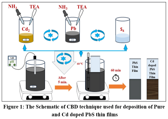 |
Figure 1: The Schematic of CBD technique used for deposition of Pure and Cd doped PbS thin films Click here to View Figure |
Results
The crystal structure of the grown thin films was characterized via a Bruker (AXS-D8 ADVANCE) X-ray diffractometer with CuKα radiation (λ = 1.5406 Å) in the 2θ range of 20°-80°. Optical studies performed by UV-Vis Spectrophotometer (Perkin-Elmer Lambda-25) within the wavelength region of 200–900nm to evaluate the absorption properties and estimate the optical bandgap. The surface morphology and microstructural characteristics were examined through field emission scanning electron microscopy (FESEM, HITACHI S-4800). Elemental analysis and successful incorporation of Cd into the PbS matrix were verified using energy-dispersive X-ray spectroscopy (EDX). In addition, density functional theory (DFT) simulations were conducted using Quantum ESPRESSO with the PBE-GGA exchange–correlation approximation to investigate the electronic structure of the films.
Discussion
XRD analysis
The X-ray diffraction (XRD) pattern of the undoped and Cd doped PbS thin film prepared by chemical bath deposition method, as illustrated in Figure 2, displays well-defined peaks corresponding to the cubic rock-salt structure of PbS. The X-ray diffraction (XRD) patterns of both undoped and cadmium (Cd)-incorporated PbS thin films clearly confirmed the successful formation of a cubic rock-salt crystal structure.16 Well-defined diffraction peaks associated with the (111), (200), and (220) crystallographic planes were distinctly identified in the diffraction patterns Upon Cd doping, The diffraction peaks demonstrated a marginal displacement towards higher 2θ angles, which can be attributed to lattice contraction arising due to to the exchange of Pb²⁺ by smaller Cd²⁺ ions. No secondary phases were detected within the instrument resolution limit. The improved crystallinity and reduced structural defects observed from XRD analysis are expected to minimize carrier recombination and enhance charge transport, thereby contributing to the enhanced photovoltaic performance of the Cd-doped PbS thin films.
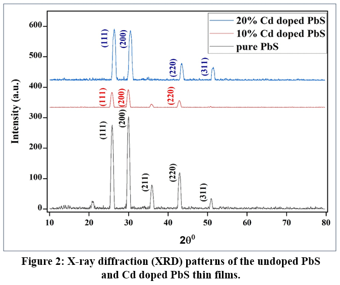 |
Figure 2: X-ray diffraction (XRD) patterns of the undoped PbS and Cd doped PbS thin films. Click here to View Figure |
The average crystallite size of the grown thin films was determined by applying the Scherrer formula, (1):
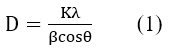
The crystallite sizes were calculated as 13.66 nm for Pure PbS, 13.45 nm for 10% Cd-PbS, and 16.32 nm for 20% Cd-PbS. Williamson–Hall analysis was performed to separate size and strain contributions. Microstrain increased at 10% doping and slightly reduced at 20%, suggesting strain relaxation at higher Cd concentration. The crystallite size ( ) and micro strain ( ) in both PbS with no Cd and PbS with Cd added. We used the Williamson-Hall (W-H) analysis to determine the film properties. The Williamson–Hall plot is derived from the equation βcosθ = (Kλ/D) + 4ε sinθ, where β is the FWHM of the diffraction peak, θ is the Bragg angle, K is the shape factor, λ is the X-ray wavelength, D is the crystallite size, and ε is the microstrain. Plotting βcosθ versus 4sinθ yields a straight line, from which the crystallite size and microstrain are extracted from the y-intercept and slope, respectively.17 The term FWHM refers to the full width at half-maximum intensity of the diffraction peak, whereas θ represents the Bragg diffraction angle. The pure PbS thin film was found to have a strain (ε) of 1.69 × 10⁻³, and the crystallite size was 13.66 nm. Upon doping with Cd (10%), the strain increased to 5.88 × 10⁻³, which corresponds to a slightly reduced crystallite size of 13.45 nm. However, with a 20% Cd doping concentration, the strain returned to 1.69 × 10⁻³, and the crystallite size increased to 16.32 nm. These observations suggest that Cd doping induces microstrain, particularly at lower doping levels (10%), which inhibits crystallite growth, as given in Figure 3 (a-b) and Figure 4 (a-b).
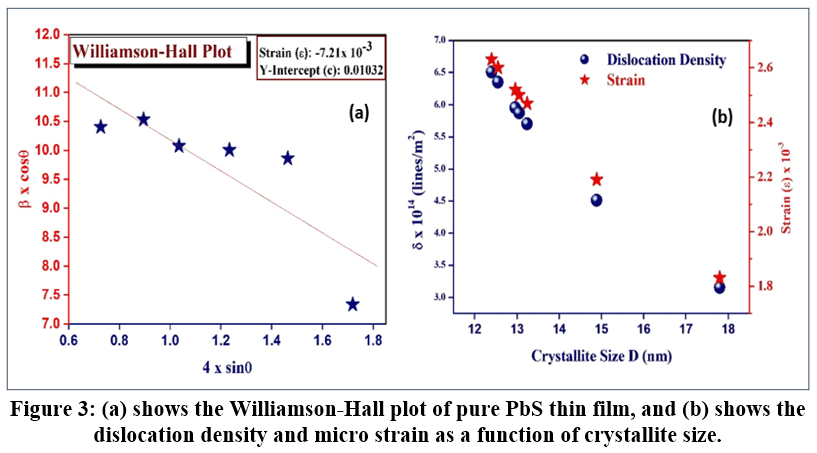 |
Figure 3: (a) shows the Williamson-Hall plot of pure PbS thin film, and (b) shows the dislocation density and micro strain as a function of crystallite size. Click here to View Figure |
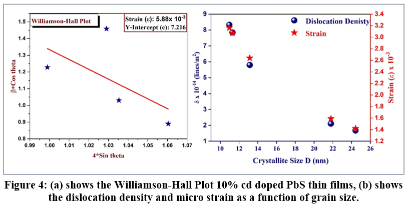 |
Figure 4: (a) shows the Williamson-Hall Plot 10% cd doped PbS thin films, (b) shows the dislocation density and micro strain as a function of grain size. Click here to View Figure |
In contrast, at greater doping levels (20%), the strain is reduced, leading to an enhancement in grain size. The crystallite sizes obtained from the Scherrer equation indicate a clear dependence on Cd doping concentration, with the 10% Cd-doped PbS film exhibiting a smaller crystallite size attributed to increased lattice strain, whereas the 20% Cd-doped film exhibited a larger crystallite size, suggesting reduced strain and improved crystallinity at higher doping levels
FESEM analysis
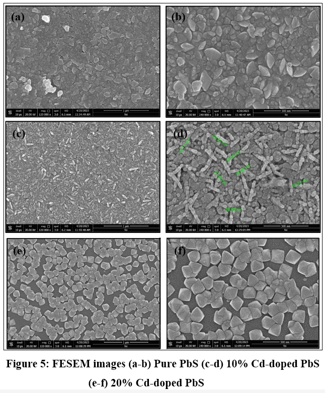 |
Figure 5: FESEM images (a-b) Pure PbS (c-d) 10% Cd-doped PbS (e-f) 20% Cd-doped PbS Click here to View Figure |
The surface morphology of undoped and Cd-incorporated PbS thin films was investigated using Field Emission Scanning Electron Microscopy (FE-SEM, Hitachi S-4800, resolution (1.0 nm at 15 kV) “Figure 5(a–f) presents the FE-SEM images of pure and Cd-doped PbS thin films deposited using varying Pb, Cd, and S precursor concentrations, captured at magnifications corresponding to 1 µm and 500 nm scale bars, revealing that the surface morphology becomes increasingly distinct with rising Cd concentration. FESEM micrographs revealed compact, uniformly distributed grains in all films. Pure PbS exhibited granular morphology. At 10% Cd doping, grains appeared relatively compact with slight elongation. At 20% Cd concentration, grain coalescence and growth were observed, resulting in comparatively larger and more uniform grains. The morphological evolution indicates that Cd doping influences surface energy and nucleation kinetics during film growth.
EDX analysis
To determine the elemental composition of the CdS thin films, energy-dispersive X-ray spectroscopy (EDX) was used. We used EDX to examine the stoichiometry of the deposited films. Deposition of CdS thin sheets with varying concentrations is shown in Figure 6, with example EDX spectra. Both Cd and S were detected; however, the relative abundances of the two varied with the amounts used to make the films. This EDX examination yielded the findings shown in Table 1. Many of the samples, such as (a, b), have relatively high cadmium concentrations, whereas others, such as (c, d), have approximately twofold higher concentrations.
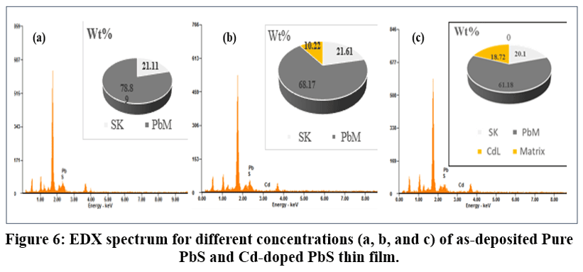 |
Figure 6: EDX spectrum for different concentrations (a, b, and c) of as-deposited Pure PbS and Cd-doped PbS thin film. Click here to View Figure |
EDX investigation confirmed the occurrence of Pb, S, and Cd in doped samples. The elemental composition showed systematic variation with increasing Cd precursor concentration, confirming successful integration of Cd into the PbS lattice. No extraneous impurity peaks were detected, indicating high film purity.
Table 1: EDX analysis details with an atomic ratio (Cd/Pb/S).
| Sr. No | Sample | Element | Wt.% | At. % |
| 1 | A | Pb | 78.89 | 63.36 |
| S | 21.11 | 36.64 | ||
| 2 | B | Cd | 10.22 | 08.32 |
| Pb | 68.17 | 30.08 | ||
| S | 21.61 | 61.60 | ||
| 3 | C | Cd | 18.72 | 18.72 |
| Pb | 61.18 | 61.18 | ||
| S | 20.10 | 20.10 |
Optical analysis
The Optical study of the pure PbS and Cd doped PbS was performed by UV visible Spectrophotometer in the wavelength range 200-1200 nm region were examined. Figure 7(a-f) Figure 7(a-f) presents the UV-Vis absorption spectra together with the corresponding Tauc plots of the pure and Cd-doped PbS thin films. The undoped PbS film displays strong absorption spanning the visible and near-infrared regions, consistent with its narrow band gap. As the Cd content increases, absorption in the visible region intensifies progressively, reaching a maximum in the 20% Cd-doped film, indicating that Cd incorporation exerts a pronounced influence on the optical absorption characteristics of the films. For each sample, the optical band gap (Eg) was extracted from the corresponding Tauc plot by evaluating the dependence of the absorption coefficient (α) on photon energy (hν). The band gap values were determined by extrapolating the linear portion of the (αhν)ⁿ versus hν curve to the point of zero absorption on the photon energy axis. The bandgap values were measured for Pure PbS (1.6 eV), 10% Cd-PbS (2.2 eV), and 20% Cd-PbS (2.4 eV).18 The increase in the bandgap with Cd doping can be attributed to modifications in the electronic band structure and to possible quantum confinement effects associated with nanoscale crystallites. The optical absorption spectra exhibited strong absorption in the visible region. The optical bandgap was determined using Tauc’s relation for direct allowed transitions as described by equation (2).

where α stands for the absorption coefficient, hν represents the photon energy, Eg corresponds to the optical band gap, and n is an integer that depends on the nature of the electronic transition. For a semiconductor with a direct band gap, n = 2, whereas for a semiconductor with an indirect band gap, n = 1/2. This relation enables a clearer understanding of the nature of the band-gap transition direct or indirect in both pure and Cd-doped PbS thin films.sssssss2,19
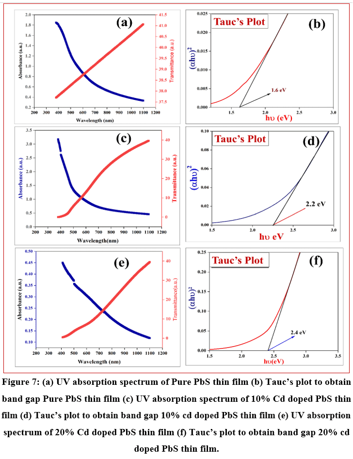 |
Figure 7: (a) UV absorption spectrum of Pure PbS thin film (b) Tauc’s plot to obtain band gap Pure PbS thin film (c) UV absorption spectrum of 10% Cd doped PbS thin film (d) Tauc’s plot to obtain band gap 10% cd doped PbS thin film |
DFT analysis
The electronic structures of bulk pristine PbS and Cd-doped PbS were obtained through quantum mechanical simulations performed in Quantum ESPRESSO, an open-source DFT package, run on a Linux platform using four 2 GHz cores and 8 GB of RAM, which proved adequate for this study. Calculations were carried out within the framework of Density Functional Theory (DFT), employing the Perdew-Burke-Ernzerhof (PBE) generalized gradient approximation (GGA) as the exchange-correlation functional, together with a plane-wave basis set. A self-consistency convergence threshold of 10⁻⁷ was applied, appropriate for accurate density of states (DOS) and band structure calculations of both PbS and Cd-doped PbS. The kinetic energy cutoffs for the wavefunction and charge density were set to 80 Ry and 300 Ry, respectively, and geometry relaxation was performed until the ionic forces fell below 0.001 eV.
The DOS and band structure of pristine bulk PbS were calculated for its face-centered cubic geometry (lattice constant 0.5936 nm), as shown in Fig. 1. The calculation yielded a Highest Occupied Molecular Level (HOMO) at 8.67 eV and a Lowest Unoccupied Molecular Level (LUMO) at 9.13 eV, corresponding to a computed energy bandgap of 0.46 eV in close agreement with the experimentally reported value of 0.41 eV. To examine the effect of Cd incorporation on the PbS lattice, a single Pb atom in the supercell was substituted with a Cd atom, as illustrated in Fig. 2. Following this substitution, the HOMO and LUMO levels shifted to 7.85 eV and 8.21 eV, respectively, corresponding to a reduced energy bandgap of 0.36 eV2.
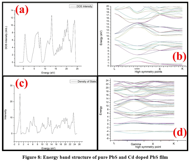 |
Figure 8: Energy band structure of pure PbS and Cd doped PbS film Click here to View Figure |
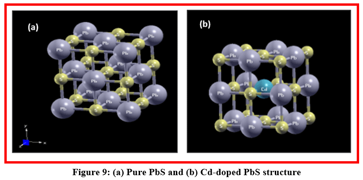 |
Figure 9: (a) Pure PbS and (b) Cd-doped PbS structure Click here to View Figure |
Conclusion
In the present work, undoped and Cd-incorporated PbS thin films were successfully grown and characterized through the chemical bath deposition (CBD) technique. XRD analysis revealed the formation of a cubic rock-salt structure in all samples, with the diffraction peaks displaying a marginal displacement towards elevated 2θ angular positions upon cadmium (Cd) substitution, attributable to lattice contraction arising from the substitutional incorporation of Cd²⁺ ions into the PbS host lattice. Crystallite size and microstrain analysis revealed doping-dependent structural modification. Optical studies demonstrated significant bandgap tuning, with values increasing from 1.6 eV for pure PbS to 2.2 eV and 2.4 eV for the 10% and 20% Cd-doped PbS films, respectively, highlighting effective band structure engineering. FESEM and EDX analyses confirmed uniform morphology and successful Cd incorporation within the PbS matrix. Density functional theory calculations further probed the electronic structure of pure and Cd-doped PbS, revealing a measurable modification of the band edges upon Cd substitution; notably, the single-atom substitution model considered here predicted a narrowing of the bandgap, in contrast to the widening observed experimentally, a divergence attributed to the dilute, isolated-defect nature of the modeled system relative to the extended substitutional doping realized in the films. The findings of the present investigation reveal that cadmium (Cd) incorporation plays a significant role in deliberately modifying the structural and optoelectronic characteristics of PbS thin films, rendering them highly suitable candidates for potential applications in photovoltaic and optoelectronic devices.
Acknowledgement
The authors express their sincere gratitude to the Department of Physics and Research Center, MGV’s MSG Arts, Science, and Commerce College, Malegaon, Maharashtra, India, for providing the necessary laboratory facilities for this research work.
Funding Sources
The author(s) received no financial support for the research, authorship, and/or publication of this article.
Conflict of Interest
The authors do not have any conflict of interest
Data Availability Statement
This statement does not apply to this article.
Ethics Statement
This research did not involve human participants, animal subjects, or any material that requires ethical approval.
Permission to Reproduce Material from Other Sources
Not applicable.
Authors’ Contribution
- Harshal Pandurang Borse: Conceptualization, methodology, investigation, experimentation, data collection, data analysis, and manuscript preparation.
- Neha Prashant Chaware: Investigation, experimental support, data analysis, and manuscript review.
- Karankumar Ramnath Sature: Experimental investigation, characterization, data interpretation, and manuscript review.
- Sajid Naeem: Data analysis, scientific interpretation, visualization, and manuscript review.
- Dhananjay Shivaji Patil: Experimental investigation, characterization, data analysis, and manuscript review.
- Umesh Jagannath Tupe: Conceptualization, supervision, scientific guidance, data interpretation, manuscript revision, and project administration.
- Nanasaheb Pandharianth Huse: Supervision, scientific guidance, experimental methodology, and critical revision of the manuscript.
- Arun Vitthal Patil: Supervision, project administration, scientific guidance, and critical review of the manuscript.
References
- Chalapathi U, Park S-H, Choi WJ. Two-step chemical bath deposition enhanced mobility of PbS thin films. Materials Science in Semiconductor Processing. 2021/12/01/ 2021;136:106147. doi:https://doi.org/10.1016/j.mssp.2021.106147
CrossRef - Alghoraibi I. Influence of the DEA Concentration on Structural and Optical Properties of Nanodot PbS Thin Films Growth by Chemical Solution Deposition: Unveiling Dual Optical Absorption Edges. Journal of Nanomaterials. 2024/01/01 2024;2024(1):9504522. doi:https://doi.org/10.1155/2024/9504522
CrossRef - Mamiyev Z, Balayeva NO. PbS nanostructures: A review of recent advances. Materials Today Sustainability. 2023/03/01/ 2023;21:100305. doi:https://doi.org/10.1016/j.mtsust.2022.100305
CrossRef - Javed A, Wahab M, Bashir M, Ahmad M, Sherazi S, Shanza. Low-cost synthesis and comprehensive characterization of Cr and Sn co-doped lead sulfide thin films for optoelectronic applications. Materials Advances. 10/20 2025;6:8586-8601. doi:10.1039/d5ma00934k
CrossRef - Madugu ML, Ahmad Makko J. Study of Cadmium Doped Lead Sulphide Thin Films Deposited Using Spray Pyrolysis Technique. Dutse Journal of Pure and Applied Sciences. 04/24 2024;10:328-336. doi:10.4314/dujopas.v10i1c.32
CrossRef - Shkir M, Palanivel B, Chandekar KV, et al. Microwave-assisted synthesis of Cu doped PbS nanostructures with enhanced dielectric and electrical properties for optoelectronic applications. Materials Science and Engineering: B. 2021/09/01/ 2021;271:115268. doi:https://doi.org/10.1016/j.mseb.2021.115268
CrossRef - Senthil E, Sangeetha R, Nirmala C, Sumathi R, Mohanasudha K. Studies on Lead Sulphide (PbS) Thin Film Prepared by Chemical Bath Deposition Method. Solid State Phenomena. 10/06 2023;350:65-73. doi:10.4028/p-oSn7M4
CrossRef - Dey T, Singh S, Jana S, Das S, Ray SK. X‑Graphene Quantum Dot/PbX (X = S, Se) Hybrid Nanostructures for Self-Powered Two-Color UV-NIR Photodetectors. ACS Applied Nano Materials. 2023;6(22):20878-20886. doi:10.1021/acsanm.3c03838
CrossRef - Ali G, Aswad T. Structure and Optical properties of Lead Sulfide (PbS) Thin Film Prepared by Chemical Bath Deposition(CBD) Technique: A Review. Journal of University of Anbar for Pure Science. 12/01 2023;17:225-233. doi:10.37652/juaps.2023.181569
CrossRef - Lv Q, Li R, Fan L, et al. High Detectivity of PbS Films Deposited on Quartz Substrates: The Role of Enhanced Photogenerated Carrier Separation. Sensors. 2023;23(20):8413. doi:10.3390/s23208413
CrossRef - Gogoi L, Chaliha S, Borah DJ, Saikia PK. Influence of Cd content on structural and optical properties of chemical bath deposited CdxPb1−xS thin films. Bulletin of Materials Science. 2021/08/07 2021;44(3):225. doi:10.1007/s12034-021-02506-2
CrossRef - Shahar B, Khan MI, Albalawi H, et al. Effect of Cd doping on the structural, optical, and photovoltaic properties of SnS films. Journal of Materials Research and Technology. 2022/07/01/ 2022;19:1982-1992. doi:https://doi.org/10.1016/j.jmrt.2022.05.137
CrossRef - Arsad AZ, Zuhdi AW, Abdullah SF, et al. Effect of Chemical Bath Deposition Variables on the Properties of Zinc Sulfide Thin Films: A Review. Molecules. 2023;28(6):2780. doi:10.3390/molecules28062780
CrossRef - Ezekoye B, Offor PO, Ezekoye V, Ezema F. Chemical Bath Deposition Technique of Thin Films: A Review. International Journal of Scientific Research. 06/01 2012;2:452-456. doi:10.15373/22778179/AUG2013/149
CrossRef - Shanza, Javed A, Ahmad M, Bashir M, Mustafa B. Insights into the microstructural, electrical, optical absorption, dispersion characteristics and hydrophobic/hydrophilic behavior of In3+ and Cd2+ co-doped lead sulfide films deposited by chemical bath deposition. Journal of Alloys and Compounds. 2026/01/15/ 2026;1050:185821. doi:https://doi.org/10.1016/j.jallcom.2025.185821
CrossRef - Faraj MG. Optimization of Thermal Budgets for Zn-Doped PbS Flexible Coatings via Chemical Spray Pyrolysis. physica status solidi (a). 2026/08/05 2026;223(15):e70476. doi:https://doi.org/10.1002/pssa.70476
CrossRef - El-Ghany W. Review on the optical and electrical properties of chalcogenide thin films: challenges and applications. Physical Chemistry Chemical Physics. 02/17 2025;27:4567-4586. doi:10.1039/d4cp04473h
CrossRef - Mamiyev Z, Balayeva N. PbS nanostructures: A Review of recent advances. Materials Today Sustainability. 03/01 2023;21:100305. doi:10.1016/j.mtsust.2022.100305
CrossRef - Shanza, Javed A, Ahmad M, Bashir M, Mustafa B. Insights into the microstructural, electrical, optical absorption, dispersion characteristics and hydrophobic behavior of In3+ and Cd2+ co-doped lead sulfide films deposited by chemical bath deposition. Journal of Alloys and Compounds. 12/01 2025;1050:185821. doi:10.1016/j.jallcom.2025.185821
CrossRef
Accepted on: 01 Sep 2026
Second Review by: Dr. Abdul Waheed Rabbani and Dr.Prajwal Chettri
Final Approval by: Dr. Oscar Jaime Restrepo Baena