High-Performance ZnO–CuO Heterojunction Thick Films for Low-Temperature Methane Sensing
 ˒Vikas Vasant Deshmane2, Umesh Jagannath Tupe3, Sajid Naeem4and Arun Vitthal Patil5*
 ¹Department of Electronic Science, MGV’s LVH Arts, Science and Commerce College, Savitribai Phule Pune University, Nashik, Maharashtra, India
2Department of Physics, SICES Degree College of Arts, Science and Commerce, University of Mumbai, Ambarnath, Maharashtra, India
3Department of Electronic Science, Vidya-Amrut Dnyan Pratishthan's Arts, Science and Commerce College, Savitribai Phule Pune University, Shirsondi, Maharashtra, India
4Department of Applied Sciences, Maulana Mukhtar Ahmad Nadvi Technical Campus, Savitribai Phule Pune University, Malegaon, Maharashtra, India
5Department of Physics, MGV’s Arts, Science and Commerce College, Savitribai Phule Pune University, Manmad, Maharashtra, India
Corresponding Author Email:aruptl@gmail.com
DOI : http://dx.doi.org/10.13005/msri/230105
Download this article as:
![]()
ZnO–CuO heterojunction thick films were developed via a screen-printing approach and systematically evaluated for low-temperature methane sensing. The formation of a p–n heterojunction between n-type ZnO and p-type CuO significantly modulates charge transport and surface reactivity. Structural analysis confirmed the coexistence of hexagonal ZnO and monoclinic CuO phases, while microstructural studies revealed a porous and well-connected morphology favorable for gas adsorption. Among all compositions, the 5 wt.% CuO–ZnO film exhibited the smallest crystallite size (~44 nm), higher defect density, and enhanced surface activity, leading to improved electronic properties with optimized resistivity and reduced activation energy. Gas sensing results demonstrated a maximum sensitivity of 94.98% toward CH₄ at a low operating temperature of 60 °C (500 ppm), along with fast response and recovery times (8 s/37 s), excellent selectivity, and long-term stability. The superior performance is attributed to the synergistic effects of increased oxygen vacancies, efficient charge transfer across the ZnO–CuO interface, and enhanced modulation of the depletion layer. These findings establish ZnO–CuO heterojunction thick films as promising candidates for energy-efficient methane sensing applications.
KEYWORDS:Material Engineering; Material Science; Methane Sensing; Screen-Printing; Thick Films; ZnO-CuO Heterojunction
Introduction
Semiconducting metal oxides (SMOs) have gained significant attention in recent years as functional materials for gas sensing applications due to their unique ability to modulate electrical conductivity upon exposure to various gaseous environments1, 2. These materials possess high chemical stability, tunable electrical and optical properties, and compatibility with low-cost fabrication techniques, making them ideal for chemiresistive sensors2-4. Among the broad family of SMOs, zinc oxide (ZnO) isindicate n-type semiconductor nature. It has direct band gap (3.3 eV) and exciton binding energy is 60 meV, has been extensively studied owing to its exceptional physicochemical stability, abundance and strong surface reactivity5, 6. ZnO is broadly employed in gas sensors, photocatalysts and optoelectronic devices. However, despite its high sensitivity, pristine ZnO suffers from certain limitations such as poor selectivity, high operating temperature and limited response–recovery behavior due to low intrinsic oxygen vacancy concentration and single-phase electron conduction mechanisms 6, 7. The various modification strategies are explored to tailor the surface and interfacial properties of ZnO7, 8. Among these, composite formation with p-type transition metal oxides (TMOs), such as CuO, NiO, and Co₃O4 has proven to be an efficient approach to enhance sensing performance9. The combination of n-type and p-type oxides leads to the formation of p–n heterojunctions, which significantly alter the charge carrier dynamics, surface potential and depletion layer width at the interface, resulting in improved sensing characteristics at lower temperatures10, 11. Among these TMOs, copper(II) oxide (CuO) has emerged as one of the most effective modifiers for ZnO due to its narrow band gap (1.2–1.9 eV), good catalytic activity, interaction with oxidizing and reducing gases, and natural p-type conductivity11, 12.The ZnO: CuO heterojunction system exhibits complementary advantages. ZnO provides high electron mobility and structural stability, while CuO contributes hole conduction and surface catalytic activity12. When these oxides are coupled, the edge between ZnO and CuO forms a depletion region that acts as an efficient barrier for charge transfer. This junction enables greater modulation of resistance upon gas adsorption and desorption, thereby enhancing sensitivity and selectivity. Moreover, the synergistic combination improves oxygen adsorption capability and electron exchange dynamics, enabling effective gas detection even at reduced operating temperatures. The sensing mechanism in such composites is primarily governed by the formation and modulation of depletion layers, oxygen vacancy concentration, and interfacial charge transfer processes11-13.
The combination of n-type and p-type metal oxides is widely reported to influence charge carrier transport through interfacial interactions, often leading to the formation of p–n heterojunction-like behavior. In the case of ZnO (n-type) and CuO (p-type), their coupling is expected to induce charge redistribution at the interface due to differences in Fermi levels, which can result in the development of a potential barrier and modulation of the depletion region 12, 13. However, in the present work, the formation of such a p–n heterojunction is inferred based on material composition and observed electrical and sensing behavior, rather than being directly confirmed through explicit electrical characterization techniques. Nevertheless, such interfacial effects are known to significantly enhance gas sensing performance by improving charge transfer dynamics and surface reactivity 13, 14.
Several researchers have reported on ZnO-CuO nanostructures prepared through sol–gel, hydrothermal, co-precipitation, and chemical vapor deposition methods. However, most of these studies have focused on thin-film or powder-based sensors, whereas thick film technology particularly based on screen-printing technique14, 15. It offers distinct advantages including uniform deposition, mechanical stability, no power required, large surface area and compatibility with scalable, low-cost sensor fabrication. Screen-printed thick films possess higher surface roughness and porosity, which play critical roles in gas diffusion and adsorption–desorption kinetics, directly influencing sensing response and recovery time. Despite these advantages, systematic studies correlating the microstructural, optical and electrical parameters of screen-printed ZnO-CuO heterojunction thick films with their gas sensing behavior remain limited in the literature15, 16.
Recent studies have shown that engineering defect chemistry and p–n heterojunction interfaces in ZnO–CuO systems significantly enhances gas sensing performance. Qi et al. (2025) demonstrated that ZnO–CuO heterostructures with abundant oxygen vacancies and internal electric fields improve charge transfer and sensing response, owing to increased active sites and efficient modulation of the depletion layer 47. Similarly, Wang, Y., (2023) and Li, S., (2024) highlight that nanostructured ZnO–CuO composites exhibit improved sensitivity due to enhanced interfacial charge transfer and catalytic activity. However, these approaches are often limited by complex synthesis routes, thin-film configurations, or high operating temperatures, restricting their practical applicability48, 49.
The present research focuses on the development and characterization of ZnO: CuO heterojunction thick films prepared by the screen-printing technique for chemiresistive gas sensing applications. The study systematically investigates the effect of CuO content on the different properties and sensing characteristics of ZnO-CuO composite films. CuO was incorporated into ZnO in varying weight percentages (1–11 wt. %), and the films were annealed at 800 °C. The incorporation of CuO is expected to modify the grain boundaries, defect density, and charge transport characteristics by introducing potential barriers at the ZnO: CuO interfaces.
Experimental Work
Materials and Methods
For the preparation of ZnO:CuO heterojunction thick films, commercially available analytical reagent (AR) grade ZnO and CuO NPs (99.99% purity) were used as starting materials. Zinc oxide served as the n-type host material, while CuO acted as the p-type additive to form the heterojunction network16, 17. Both oxides were used without further purification. Alumina substrates were used as the supporting base for thick film deposition due to their high thermal stability, good adhesion characteristics and electrical insulation properties. Before the preparation of films, the alumina substrates were thoroughly cleaned in acetone to remove organic and particulate contaminants. The cleaned substrates kept underIR lamp irradiation for 15-20 minutes, to ensure complete removal of residual solvents and moisture, thus providing a clean and uniform surface for film formation17, 18.
Preparation of ZnO-CuO paste
The composite formulation for thick film preparation was designed on a 70:30 weight ratio basis, where 70% constituted the ZnO–CuO nanoparticle mixture and 30% comprised the organic–inorganic binders. For a typical 1 g paste, 0.70 g of ZnO–CuO powder mixture and 0.30 g of binder (0.024 g ethyl cellulose and 0.276 g BCA) were used. The CuO content was varied from 1 to 11 wt.% by adjusting the ZnO:CuO ratio accordingly.The binders consisted of butyl carbitol acetate (BCA) as a solvent and ethyl cellulose (EC) as an organic binder, which provided suitable viscosity, adhesion, and thixotropic behavior to the paste.To systematically examine the influence of CuO incorporation, six different composite formulations were prepared with CuO contents of 1, 3, 5, 7, 9 and 11 wt.%, each blended with ZnO as the host matrix19.Within the 0.70 g inorganic fraction, the CuO content was varied as 1, 3, 5, 7, 9, and 11 wt.% relative to ZnO. In the optimized 5 wt.% CuO composition, 0.665 g ZnO and 0.035 g CuO were used. Similarly, for 1 wt.% CuO: 0.693 g ZnO + 0.007 g CuO; for 3 wt.%: 0.679 g ZnO + 0.021 g CuO; for 7 wt.%: 0.651 g ZnO + 0.049 g CuO; for 9 wt.%: 0.637 g ZnO + 0.063 g CuO; and for 11 wt.%: 0.623 g ZnO + 0.077 g CuO. The powders and binders were thoroughly merge by mortar and pestle for approximately 30–40 minutes until a homogeneous and smooth thixotropic paste was obtained. This meticulous manual mixing ensured uniform dispersion of CuO nanoparticles within the ZnO matrix and consistent rheological behavior of the paste, essential for reproducible screen printing19, 20.
Preparation of films
Films of ZnO: CuO were prepared by standard screen-printing technique. The prepared ZnO: CuO paste was placed onto the pre-cleaned alumina substrates, which enables the controlled deposition of uniform and reproducible films over large areas. Stainless steel mesh screens of regular mesh size were used to achieve precise film thickness and pattern uniformity. Films were kept under IR radiation for 25 minutes to eliminate residual solvent (BCA) and eliminate possible contaminants. This step was crucial to prevent bubble formation and surface irregularities during the subsequent high-temperature treatment. Using muffle furnace at 800 °C for 3 hours films were annealed. Annealed ZnO: CuO composite thick films exhibited strong mechanical adhesion, good surface uniformity and were ready for further characterization18-20. Film thickness was estimated using mass difference method, the thickness of prepared films was found to be in micrometer range as tabulated in Table 3.
Characterization of ZnO-CuO thick films
Annealed ZnO:CuO films characterized by a combination of advanced analytical, optical, and electrical techniques to comprehensively evaluate their structural, morphological and functional properties. The structural properties and phase purity of the films were analyzed using XRD with a Bruker D8 VENTURE. XRD measurements were carried out using Cu Kα radiation (λ = 1.5406 Å) over a 2θ scan range of 20°–80°, with a step size of 0.02° and an appropriate scanning rate. Surface morphology was studied by FE-SEM using a FEI Nova NanoSEM 450, while elemental composition was confirmed through EDX with a Bruker XFlash 6I30 detector. FESEM analysis was performed at an accelerating voltage of 10–15 kV to examine the surface morphology, while EDX analysis was conducted for elemental composition using an attached detector under similar operating conditions. FTIR analysis using a PerkinElmer Spectrum Two identified chemical bonding, and optical properties were examined with a Shimadzu UV-2600 spectrophotometer. FTIR spectra were recorded in the wavenumber range of 400–4000 cm⁻¹ using the standard transmittance mode to identify characteristic functional groups and metal–oxygen vibrations. UV–Visible spectroscopy measurements were carried out in the wavelength range of 200–800 nm to determine the optical absorption behavior and band gap of the films. Electrical parameters were measured using the half-bridge method21, 22. The gas sensing parameters such as sensitivity, selectivity, response time and recovery time, were determined for various target gases, including methane (CH4), nitrogen dioxide (NO₂), liquefied petroleum gas (LPG), sulfur dioxide (SO₂), ethanol and methanol, over a wide concentration range of 100–1000 ppm and at operating temperatures between 30 and 150 °C.
Results
The XRD patterns of ZnO:CuO films (1–11 wt.% CuO) show sharp and well-defined peaks, confirming their crystalline nature. The diffraction peaks at 2θ ≈ 31.7°, 34.4°, 36.2°, 47.5°, 56.6°, 62.9°, 67.9°, and 69.1° correspond to the (100), (002), (101), (102), (110), (103), (112) and (201) planes of hexagonal wurtzite ZnO (JCPDS Card No. 36-1451). In addition to ZnO peaks, other diffraction peaks appearing at around 32.5°, 35.6°, 38.7°, 48.7°, 53.5°, 65.8°, 67.9°, and 72.4° are indexed to the (110), (002), (111), (020), (202), (220), (112) and (004) planes of monoclinic CuO (JCPDS Card No. 02-1041) 23, 24.
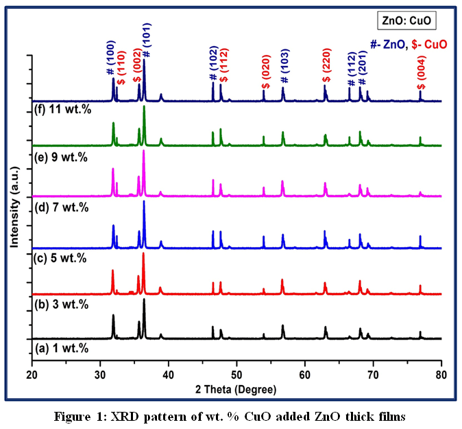 |
Figure 1: XRD pattern of wt. % CuO added ZnO thick films Click here to View Figure |
The relative variation in peak intensities with increasing CuO content indicates microstructural modifications within the ZnO matrix. The (002) diffraction peak of ZnO, associated with preferential growth along the c-axis, remains nearly unchanged across different compositions, suggesting that the dominant growth orientation of ZnO crystallites is largely preserved even after CuO incorporation. In contrast, variations in the intensity of other planes, such as (110), can be attributed to changes in crystallite orientation, lattice strain, and the increasing contribution of CuO phases at higher concentrations. The incorporation of CuO nanoparticles introduces localized distortions and modifies grain growth dynamics, which in turn affects the relative intensity distribution of diffraction peaks.
The coexistence of both ZnO and CuO phases in the diffraction profiles confirms the successful construction of a ZnO: CuO heterojunction composite without the appearance of any impurity peaks, indicating good chemical compatibility between the two oxides. Using the Debye–Scherrer equation (Eq. 1), crystallite size was estimated 14, 23.
Where,
D- Crystallite size, K- Scherrer constant (0.9), β – FWHM, and λ – Wavelength of X source.
The crystallite sizes of ZnO:CuO films were calculated as 52, 51, 44, 48, 49 and 49 nm for 1, 3, 5, 7, 9, and 11 wt.% CuO, respectively. The 5 wt.% CuO-doped film showed the smallest size (44 nm), likely due to uniform dispersion of CuO within the ZnO matrix. CuO content exceeds 5 wt.%, agglomeration of CuO particles takes place, reducing their uniform distribution and pinning efficiency12, 14. This promotes localized grain coarsening and results in an increase in crystallite size for 7–11 wt. % samples. Excess CuO also enhances diffusion and sintering kinetics, leading to the merging of grains and a slight increase in crystallite size.
Crystallite size significantly affects the gas sensing performance of ZnO:CuO heterojunction films. Smaller crystallites provide a higher surface-to-volume ratio, increasing active sites for gas adsorption and improving sensor response. When the grain size is comparable to or smaller than twice the Debye length, the entire grain participates in charge modulation, leading to enhanced sensitivity and faster response 11, 14. The smaller crystallites enhance the density of grain boundaries and p–n junction interfaces, which are highly sensitive to surface charge variations upon gas exposure. Table 1 shows XRD parameters of films.
Table 1: XRD parameters of ZnO: CuO thick films
| Wt. % CuO additive | 2 Theta
(Degree) |
FWHM
(Degree) |
Crystallite size
(nm) |
| 1 wt.% | 36.34 | 0.1664 | 52 |
| 3 wt.% | 36.43 | 0.1693 | 51 |
| 5 wt.% | 36.44 | 0.1663 | 44 |
| 7 wt.% | 36.35 | 0.1802 | 48 |
| 9 wt.% | 36.48 | 0.1796 | 49 |
| 11 wt.% | 36.42 | 0.1753 | 49 |
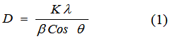
FE-SEM was used to study the surface morphology of films with 1–11 wt.% CuO (Fig. 2 a–f).The micrographs clearly reveal that all samples exhibit a porous and granular surface morphology with well-connected grains, confirming that the screen-printing and subsequent annealing processes led to the formation of compact yet porous thick films. The morphology and grain connectivity are significantly influenced by the CuO concentration in the ZnO matrix. At 1 wt. % CuO (Fig. 2a), the film surface shows irregular, densely packed grains with limited porosity and fewer voids, indicating incomplete intergranular connectivity 14, 15. The 3 wt. % CuO sample (Fig. 2b) shows improved surface uniformity and slightly increased porosity due to better dispersion of CuO nanoparticles, which hinder the excessive agglomeration of ZnO grains. The most uniform and well-developed porous morphology is observed for the 5 wt. % CuO film (Fig. 2c), which exhibits homogeneously distributed grains, well-defined voids, and enhanced porosity. This morphology suggests that CuO nanoparticles at this concentration are optimally dispersed within the ZnO matrix, acting as effective barriers to grain coalescence and thereby creating numerous nanoscale voids and intergranular boundaries. The 7 wt. % CuO film (Fig. 2d) begins to exhibit partial agglomeration of grains with a reduction in porosity, while at higher CuO concentrations of 9 wt. % and 11 wt. % (Fig. 2e–f), significant grain coarsening and agglomeration are evident. The quantitative image analysis has been performed using ImageJ software to support the qualitative observations. Key morphological parameters such as surface porosity, average grain size, and degree of agglomeration were estimated from the FE-SEM images. The analysis confirms that the 5 wt.% CuO–ZnO film exhibits the highest porosity and most uniform grain distribution, while higher CuO concentrations (≥7 wt.%) show increased agglomeration and reduced pore connectivity.
 |
Figure 2: FE-SEM micrograph of wt. % CuO added ZnO thick films Click here to View Figure |
The excess CuO leads to the formation of larger clusters, decreasing the number of open pores and thereby reducing the overall porosity and surface area of the films.Specific surface area (SSA) of films was calculated using the BET method (Eq. 2) 25.
Where, Sw -Specific surface area, d – Diameter of the spherical particles, and ρ – composite density.
The specific surface area (SSA) of the films was estimated using a simplified relation based on particle size and density. The calculated SSA values were approximately 3.4, 3.5, 5.8, 4.3, 3.7 and 3.7 m²/gfor 1–11 wt.% CuO-doped ZnO films, respectively, with the highest value observed for the 5 wt.% CuO composition, with the highest value (5.8m²/g) observed for 5 wt.% CuO, which correlates well with the FESEM observations of a highly porous and uniformly distributed grain structure. The enhanced specific surface area and porosity at 5 wt. % CuO arise due to the synergistic effect of ZnO: CuO interfacial interactions and controlled grain growth inhibition. Specific surface area and porosity strongly influence gas sensing performance. Higher surface area increases active sites for gas adsorption, enhancing the amount of chemisorbed oxygen species (O⁻, O₂⁻, O₂⁻²) on the sensor surface26, 27. The presence of more adsorbed oxygen enhances the modulation of surface charge and electrical resistance upon exposure to target gases, resulting in a higher sensing response. The porous, interconnected structure enables efficient gas diffusion, promoting rapid interaction with active sites and resulting in faster response and recovery times 28. The films with lower porosity and surface area limit gas penetration, causing slower kinetics and reduced sensitivity27, 28.
EDX was used to analyze the elemental composition of films and the corresponding spectra and elemental data are presented in Fig. 3(a–f) and Table 1, respectively. The EDX spectra clearly show the characteristic peaks of Zn, Cu, and O, confirming the presence of the expected constituent elements without any impurity signals, which indicates the chemical purity of the prepared samples. The weight percentage data reveal that the relative proportions of Zn, Cu, and O vary with increasing CuO content, demonstrating that CuO incorporation influences the overall elemental distribution and stoichiometry of the films14, 19, 25. Among the analyzed samples, the 5 wt. % CuO-added ZnO film shows a significantly reduced oxygen content (2.11 wt.%), suggesting a higher degree of oxygen deficiency compared to other compositions.
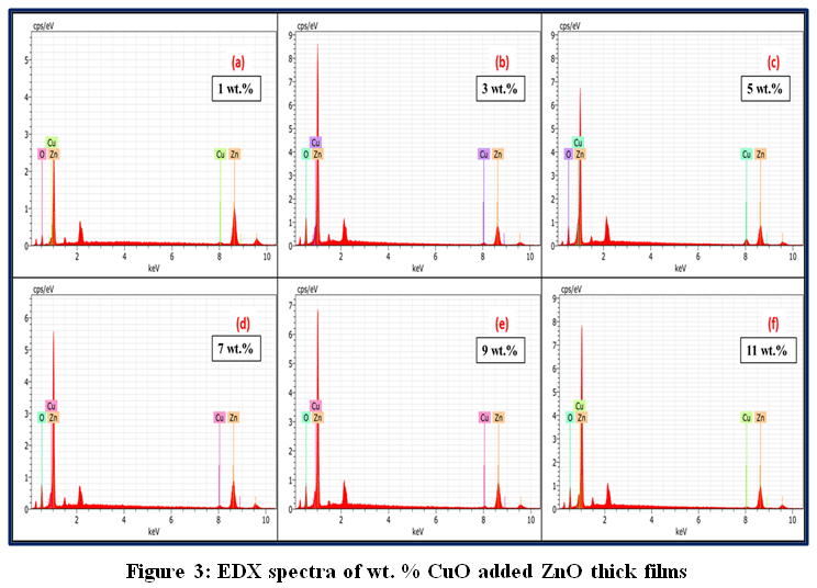 |
Figure 3: EDX spectra of wt. % CuO added ZnO thick films Click here to View Figure |
The oxygen deficiency in the 5 wt.% CuO-doped ZnO film enhances gas sensing performance, as oxygen vacancies act as electron donors, improving carrier concentration and surface reactivity. These vacancies serve as active sites for chemisorption of oxygen species (O₂⁻, O⁻, O²⁻) when the sensor is exposed to air, leading to the formation of a surface depletion layer25, 27. Quantitative elemental analysis of ZnO: CuO films is demonstrated in Table 2.
Table 2: Quantitative elemental analysis of ZnO: CuO thick films
| Wt. % CuO additive | EDX analysis (Weight %) | ||
| Zn | Cu | O | |
| 1 wt.% | 78.87 | 5.69 | 15.44 |
| 3 wt.% | 85.39 | 5.55 | 9.06 |
| 5 wt.% | 96.23 | 1.66 | 2.11 |
| 7 wt.% | 90.73 | 2.69 | 6.58 |
| 9 wt.% | 89.68 | 3.51 | 6.81 |
| 11 wt.% | 90.17 | 3.72 | 6.11 |
The FTIR spectra of the ZnO: CuO thick films (Fig. 4) show the expected metal–oxygen vibrational region and weaker high-wavenumber bands. All samples exhibit pronounced absorption in the region in between 400–700 cm⁻¹ that could be attributed to metal–oxygen stretching modes.The Zn–O vibrations of the wurtzite lattice typically appear near ≈430–520 cm⁻¹, while Cu–O vibrations of monoclinic CuO are found at somewhat higher wavenumbers (often ≈530–600 cm⁻¹); small shifts, shoulders, and band broadening arise from heterojunction formation, lattice strain, and particle size effects. Weak, broad bands in the region ≈3200–3600 cm⁻¹ and a bending band near ≈1600–1650 cm⁻¹ indicate surface –OH groups and physisorbed water; very small features around 2800–3000 cm⁻¹ can be attributed to residual organics from binders if present14, 31.
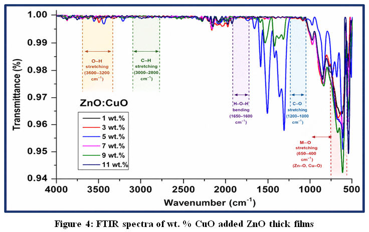 |
Figure 4: FTIR spectra of wt. % CuO added ZnO thick films Click here to View Figure |
For a gas sensing purpose these FTIR observations matter because oxygen vacancies and lattice defects (inferred from M–O band broadening and shifts) act as active adsorption centers for atmospheric molecules; they enhance chemisorption, promote charge transfer and increase the modulation of the barrier potential at the ZnO: CuO p–n interfaces31, 32. The reduced hydroxyl/organic coverage improves accessibility of these active sites and speeds adsorption/desorption kinetics. When combined with the corroborating FESEM (higher porosity, interconnected voids) and EDX (oxygen deficiency) results for the 5 wt. % sample, the FTIR data thus support the conclusion that 5 wt. % CuO produces an optimal surface chemistry and defect structure for chemiresistive gas sensing more active adsorption sites, efficient charge exchange at heterojunctions, and faster response/recovery whereas lower CuO gives fewer defects and higher loadings lead to agglomeration/overcoverage that reduce active surface availability25, 26. The broad absorption band observed in the region of 3200–3600 cm⁻¹ is generally attributed to O–H stretching vibrations of surface hydroxyl groups and/or adsorbed moisture. However, contributions from residual carbon-containing species or atmospheric contamination cannot be completely excluded. Since the FTIR measurements were performed under ambient conditions, re-adsorption of moisture on the film surface after high-temperature annealing is likely 3, 27.The films were annealed at 800 °C in air and subsequently exposed to ambient conditions prior to FTIR analysis. Therefore, the presence of surface hydroxyl groups is attributed to post-annealing atmospheric adsorption rather than retained species from the annealing process3, 27, 32.
The UV–Vis spectra of films show a strong absorption edge at ~350–390 nm, corresponding to the band-to-band transition of ZnO; superimposed on this edge are weak long-wavelength tails and slight variations in the edge position and slope that reflect the influence of CuO addition, interfacial defects and sub-bandgap states30, 31. The 5 wt. % CuO sample exhibits the most favourable optical signature for chemiresistive sensing, its absorption edge remains sharp while showing a modest increase in sub-bandgap absorbance compared with the low (1–3 wt.%) and high (7–11 wt.%) CuO thick films. This extra sub-bandgap absorption is consistent with an increased density of defect states (oxygen vacancies and interfacial states) and stronger ZnO: CuO interaction at the heterojunctions31, 32.
The estimated optical band gap values for all compositions are approximately ~3.1 eV, with only minor variations observed. These small differences fall within the experimental uncertainty of the Tauc method and therefore should be interpreted cautiously. The band gap of ZnO:CuO films, estimated from Tauc plots, was 3.12, 3.16, 3.09, 3.03, 3.14 and 3.11 eV for 1–11 wt.% CuO respectively. These results indicate that the energy band gap slightly varies with the CuO concentration, reflecting modifications in the electronic structure due to CuO incorporation and ZnO: CuO heterojunction formation.
![]()
Where,
Eg is the optical band gap energy, α is the absorption coefficient of the material, hν is the photon energy, A is a proportionality constant and n is electronic transition.
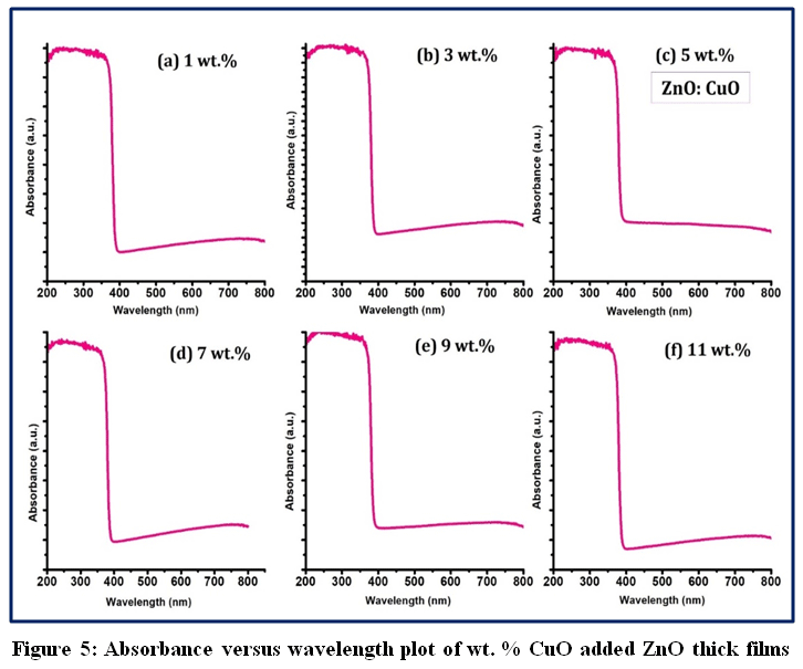 |
Figure 5: Absorbance versus wavelength plot of wt. % CuO added ZnO thick films Click here to View Figure |
The 5 wt. % CuO added ZnO film exhibits a slightly lower band gap value (3.09 eV) compared to other compositions, indicating enhanced electronic coupling and defect formation at the ZnO: CuO interface 12, 33. The band gap reduction is due to defect levels near the conduction band formed by lattice distortion and oxygen vacancies from Cu²⁺ incorporation, enabling easier electronic transitions and causing a redshift in absorption 34. A smaller band gap improves electrical conductivity and carrier mobility, enabling easier electron excitation. This enhances charge transfer during gas adsorption, leading to a stronger sensor response through effective modulation of carrier concentration 34, 35.
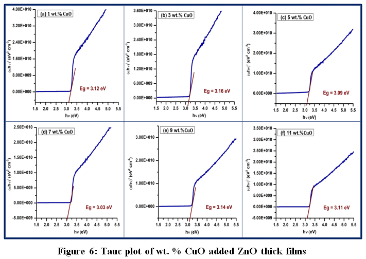 |
Figure 6: Tauc plot of wt. % CuO added ZnO thick films Click here to View Figure |
A narrower band gap promotes stronger light absorption and enhances surface photoactivation, which also impact in desorption and regeneration processes during sensing, improving response and recovery times.
It is clarified that the slight reduction in band gap observed for the optimized 5 wt.% CuO composition is primarily due to the introduction of defect states (such as oxygen vacancy-related levels) and strong electronic coupling at the ZnO–CuO interface, which create localized energy levels near the conduction band and facilitate easier electronic transitions. In contrast, at higher CuO concentrations (≥7 wt.%), the band gap variation is influenced by particle agglomeration and reduced effective interfacial interaction, leading to less pronounced defect-mediated band tailing.
The electrical behavior of ZnO: CuO thick films was studied through resistance–temperature (R–T) and logarithmic resistance versus inverse temperature (log Rc–1/T) plots, as shown in Fig. 7(a) and (b). The R–T characteristics in Fig. 7(a) reveal that the electrical resistance of all films decreases exponentially with increasing temperature, confirming their semiconducting nature25, 36. This behavior arises due to the thermally activated conduction mechanism, where an increase in temperature provides sufficient energy to excite more electrons from localized states into the conduction band, thus enhancing conductivity36, 37.
The observed variation in film thickness with increasing CuO content is primarily attributed to changes in the rheological properties of the screen-printing paste. The incorporation of CuO nanoparticles modifies the viscosity, particle packing density, and thixotropic behavior of the ZnO-based paste, thereby influencing the amount of material deposited during the printing process. As a result, slight variations in film thickness are expected even under controlled fabrication conditions form Table 3. The electrical properties of the ZnO–CuO thick films were evaluated in terms of resistivity, temperature coefficient of resistance (TCR), and activation energy. The resistivity values were found to be on the order of ~10⁵ Ω·m for all compositions, showing a general variation with CuO content. However, it is important to note that resistivity measurements in thick films are subject to uncertainties arising from factors such as thickness measurement errors, contact resistance, and film inhomogeneity.
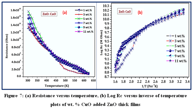 |
Figure 7: (a) Resistance versus temperature, (b) Log Rc versus inverse of temperature plots of wt. % CuO added ZnO thick films Click here to View Figure |
Electrical characterization was performed using the half-bridge method, evaluating resistivity, Temperature Coefficient of Resistance (TCR), and activation energy at different temperature regions using Eqs. 4–6 36, 37.
Where,
ρ – Resistivity of prepared film, R- Resistance at normal temperature, b – Breadth of film,
t – Thickness of the film, L – Length of the film.
Where,
∆R – Change in resistance, ∆T – Temperature difference, and Ro – Initial resistance of the film.
![]()
Where,
ΔE – Activation energy, R- Resistance at raised temperature, R0 – Resistance at room temperature.
The variation of resistivity, TCR, and activation energy (Eₐ) for films with different CuO concentrations is shown in Fig. 8 (a–c).
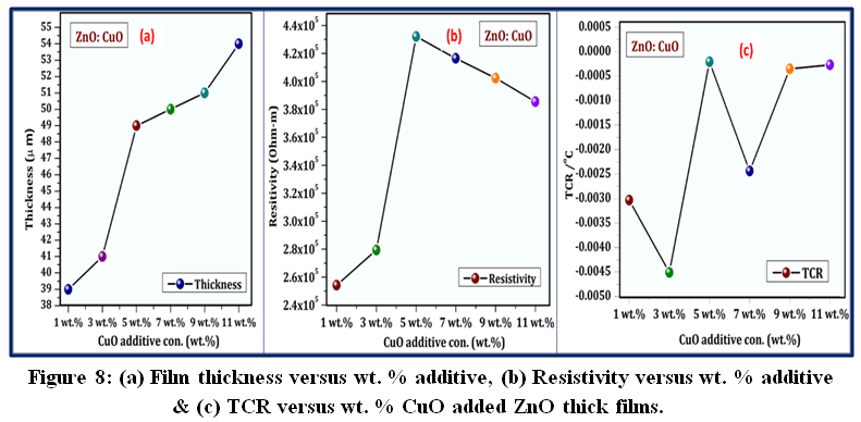 |
Figure 8: (a) Film thickness versus wt. % additive, (b) Resistivity versus wt. % additive &(c) TCR versus wt. % CuO added ZnO thick films. Click here to View Figure |
The resistivity values tabulated in Table 3. The results indicate that the electrical resistivity increases with CuO concentration up to 5 wt.%, after which it slightly decreases. This trend can be attributed to the interplay between microstructural evolution and interfacial charge transport within the ZnO: CuO heterojunction network. At lower CuO concentrations (1–3 wt.%), The CuO content is too low to form an effective p–n junction network with ZnO, resulting in relatively lower resistivity. As the CuO content increases to 5 wt.%, numerous p–n heterojunctions are formed at the ZnO: CuO interfaces, which enhance the potential barrier height and reduce the free carrier concentration, thereby increasing resistivity. Beyond 5 wt. % CuO, the excessive CuO tends to agglomerate and form larger clusters that disrupt the uniform distribution of heterojunctions, creating alternative conduction paths and slightly lowering the resistivity values for 7–11 wt. % samples.The TCR values for all the ZnO: CuO films were found to be negative, confirming their semiconducting nature, as the resistance decreases with increasing temperature37, 38.The activation energy (Eₐ), derived from Arrhenius plots of log R vs. 1/T, also shows a strong dependence on CuO content. Activation energy was estimated in two conduction regions, a low-temperature region (LTR) dominated by hopping or defect-assisted conduction, and a high-temperature region (HTR) governed by thermally activated band conduction. The activation energy decreases up to 5 wt. % CuO and then increases slightly at higher concentrations. This reduction in Ea at 5 wt. % indicates that less energy is required for charge carriers to overcome potential barriers, which enhances carrier mobility and interfacial conduction. The optimized Ea value at this concentration is attributed to the formation of well-dispersed ZnO: CuO heterojunctions, which facilitate efficient charge separation and electron transport across the interface. When CuO concentration exceeds 5 wt.%, the agglomeration of CuO grains leads to non-uniform interfaces and increased scattering centers, resulting in a higher activation energy31, 37.
Discussion
Gas sensing was studied using a static system, with sensitivity and selectivity evaluated using Eqs. 7 and 838, 39.
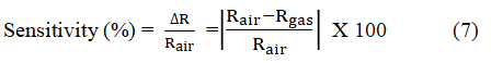
Where, Ra = resistance in air and Rg = resistance in the presence of gas
The electrical results of CuO-added ZnO thick films are summarized in Table 3.
Table 3: Electrical outcomes of CuO-added ZnO thick films.
| Thick Film | Thickness
(µm) |
Resistivity
(Ω.m) |
TCR
(oC-1) |
Activation energy ( eV) | |
| LTR | HTR | ||||
| 1 wt.% | 39 | 2.8× 10⁵ | -0.0030 | 0.1193 | 0.0368 |
| 3 wt.% | 41 | 2.4× 10⁵ | -0.0045 | 0.3643 | 0.071 |
| 5 wt.% | 49 | 4.9× 10⁵ | -0.0002 | 0.0967 | 0.0914 |
| 7 wt.% | 50 | 4.6× 10⁵ | -0.0024 | 0.1286 | 0.1021 |
| 9 wt.% | 51 | 4.5× 10⁵ | -0.0004 | 0.1257 | 0.0586 |
| 11 wt.% | 54 | 3.2× 10⁵ | -0.0003 | 0.0846 | 0.1641 |
The gas sensing analysis of films with varying CuO concentrations (1–11 wt.%) toward different target gases (CH4, NO₂, LPG, SO₂, ethanol, and methanol) at various operating temperatures is shown in Fig. 9(a–f). Among the investigated gases, all films exhibit the highest sensitivity toward methane (CH4). The maximum sensitivity to CH4 gas was found to be 62.35%, 75.01%, 94.98%, 88.52%, 72.41%, and 81.67% for 1 wt.%, 3 wt.%, 5 wt.%, 7 wt.%, 9 wt.%, and 11 wt. % CuO-added ZnO thick films respectively, measured at an optimum operating temperature of 60 °C and a CH4 gas concentration of 500 ppm.
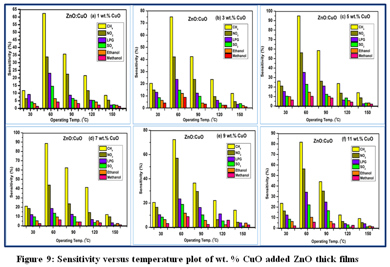 |
Figure 9: Sensitivity versus temperature plot of wt. % CuO added ZnO thick films Click here to View Figure |
The results clearly indicate that the 5 wt. % CuO-added ZnO film exhibits the highest sensitivity (94.98%), significantly higher than other compositions, suggesting that this sample possesses the most favorable microstructural, electrical, and surface properties for gas sensing applications 37-40. The superior gas sensing behavior of the 5 wt. % CuO added ZnO thick film could be attributed due to its optimized microstructure, defect density and electrical properties, which work synergistically to enhance the gas–solid interaction process. Structural characterization (XRD) confirmed that the 5 wt. % film exhibits a smallest crystallite size (~44.41 nm) among all compositions. The reduced crystallite size leads to a higher s/v, providing more active sites for oxygen and gas molecule adsorption 25, 39. The FESEM analysis revealed that this composition also possesses uniformly distributed grains, high porosity, and abundant surface voids, which facilitate faster diffusion and adsorption of gas molecules into the sensing layer. These morphological features play a crucial role in determining the sensing response, as they directly influence the amount of adsorbed oxygen species (O⁻, O₂⁻, O²⁻) that participate in redox reactions with CH4 molecules. EDX results demonstrated a relatively oxygen-deficient structure in the 5 wt. % sample, which further enhances sensing performance 15, 41.Oxygen vacancies act as electron donors, enhancing oxygen adsorption and ionization. Upon exposure to CH4, the gas reacts with adsorbed oxygen ions, releasing electrons back to the conduction band, decreasing resistance and increasing sensor response. The presence of an optimum number of oxygen vacancies in the 5 wt. % film ensures that sufficient oxygen species are available for surface reactions, while preventing excessive defect accumulation that could hinder charge mobility, as seen in higher CuO concentrations (7–11 wt.%).Electrical characterization also supports the superior performance of the 5 wt. % CuO sample. It exhibited highest resistivity (4.32 × 10⁵ Ω·m), higher negative TCR and lowest activation energy among all compositions, indicating efficient charge carrier transport and rapid response to surface reactions. The presence of numerous well-distributed p–n heterojunctions between n-type ZnO and p-type CuO enhances the charge transfer process at the interface12-14. Upon gas exposure, the depletion region at the p–n junction is modulated significantly due to electron exchange between the adsorbed gas and the sensing layer, resulting in a pronounced change in resistance. This interfacial modulation is most efficient in the 5 wt. % CuO film because of its balanced composition sufficient CuO to form numerous active junctions.In contrast, films with lower CuO concentrations (1–3 wt.%) contain fewer CuO nanoparticles and consequently fewer p–n junctions, leading to weaker modulation of resistance and lower sensitivity. On the other hand, higher CuO loadings (7–11 wt.%) result in aggregation of CuO clusters, which decreases the effective surface area, increases recombination losses, and reduces the interfacial charge transfer efficiency, leading to diminished gas response. Therefore 5 wt. % CuO added ZnO thick film demonstrates an ideal balance between crystallite size, porosity, oxygen vacancy concentration, and p–n junction density, all of which contribute to its exceptional methane gas sensing characteristics2-4. The optimized structural and electrical features enable a high sensitivity of 94.98% at a low operating temperature (60 °C), making this composition highly efficient, energy-saving, and suitable for practical gas sensing applications.
The gas sensing recital of the 5 wt. % CuO-added ZnO thick film toward CH4 and other selected gases is illustrated in Fig. 10 (a–d), which highlights the sensor’s sensitivity, selectivity, reusability, and response–recovery behavior. The results demonstrate that this composition exhibits superior gas sensing characteristics compared to other CuO concentrations, confirming it as the most efficient formulation for CH4 detection. The sensitivity versus CH4 gas concentration plot Fig. 10(a) shows that the sensitivity increases with rising CH4 concentration up to 500 ppm, after which it begins to saturate. The sensitivity values were 23.58%, 51.29%, 94.98%, 88.41%, and 90.23% for CH4 gas concentrations of 100, 300, 500, 700 and 1000 ppm respectively, at an optimum operating temperature of 60 °C. The increase in sensitivity up to 500 ppm can be attributed to the greater availability of CH4 molecules that react with the surface-adsorbed oxygen species (O⁻ and O₂⁻) on the ZnO–CuO film, releasing trapped electrons back to the conduction band and thus decreasing the film’s resistance 33, 36. Beyond 500 ppm, the sensitivity tends to plateau because the number of available oxygen adsorption sites becomes limited, resulting in saturation of the sensor response. The high sensitivity (94.98%) at 500 ppm indicates efficient surface reactions and rapid charge transfer due to the optimized heterojunction network and high density of active sites in the 5 wt. % CuO–ZnO composite.
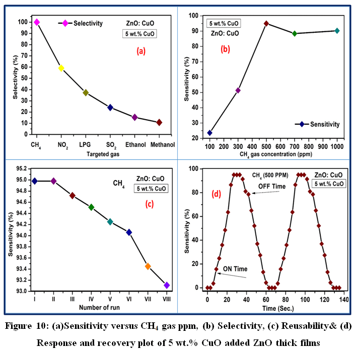 |
Figure 10: (a)Sensitivity versus CH4 gas ppm, (b) Selectivity, (c) Reusability& (d) Response and recovery plot of 5 wt.% CuO added ZnO thick films |
The selectivity plot Fig. 10 (b) demonstrates that the 5 wt. % CuO–ZnO thick film exhibits the highest response to CH4 compared to other target gases such as NO2, LPG, SO2 ethanol and methanol with selectivity values of 100%, 59.09%, 37.28%, 24.05%, 15.32% and 10.77%, respectively.
The pronounced selectivity toward CH4 is mainly due to the specific interaction mechanism between methane molecules and surface oxygen species, which effectively alters the depletion layer at the ZnO: CuO p–n junction. Which releases electrons that reduce the potential barrier at the ZnO–CuO interface, causing a large change in resistance and thus a high sensitivity 4, 36. The lower responses to other gases can be attributed to differences in their adsorption energy, chemical affinity, and reaction kinetics with surface oxygen species, confirming the excellent chemical selectivity of the optimized film toward CH4.The reusability or long-term stability test Fig. 10(c) shows that the 5 wt. % CuO–ZnO sensor maintains excellent repeatability over eight consecutive runs (one run per day for eight days). The sensitivity values slightly decreased from 94.98% in the first two runs to 93.11% in the eighth run, indicating minimal degradation in performance over time38, 39. This excellent reusability and stability could be attributed to the strong adhesion of the film on the substrate, the thermal robustness of ZnO: CuO composites, and the stable p–n heterojunction interfaces that maintain consistent electron transfer during repeated adsorption–desorption cycles. Such stability is crucial for practical sensor deployment in continuous or long-term gas monitoring systems.The response and recovery plot Fig. 10(d) reveals that the 5 wt. % CuO–ZnO thick film exhibits an extremely fast response time of 8 seconds and a recovery time of 37 seconds toward 500 ppm CH4 gas at 60 °C. The short response time indicates rapid adsorption and surface reaction of CH4 molecules with the pre-adsorbed oxygen ions, leading to an immediate change in resistance 36-38. The relatively quick recovery time demonstrates efficient desorption of reaction products (CO₂ and H₂O) and re-adsorption of oxygen molecules when the gas flow is switched off. This fast dynamic behavior can be ascribed to the high surface porosity, uniform grain distribution, and optimal CuO loading, which enable rapid gas diffusion and electron exchange within the sensing layer39-41.
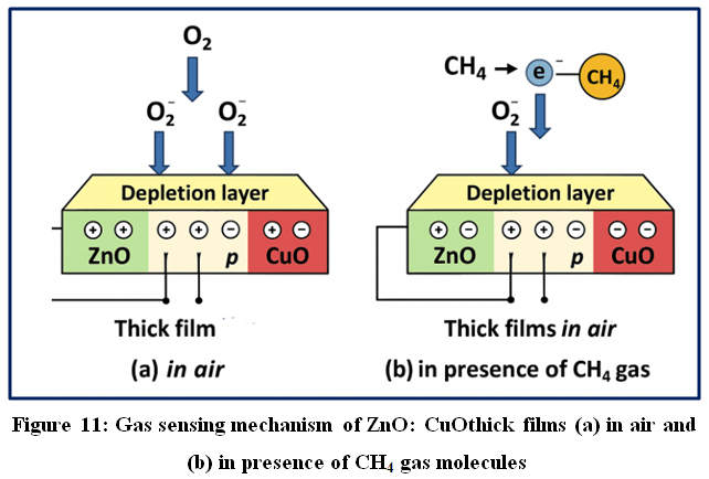 |
Figure 11: Gas sensing mechanism of ZnO: CuOthick films (a) in air and (b) in presence of CH4 gas molecules Click here to View Figure |
The gas sensing mechanism of ZnO:CuO thick films (Fig. 11) is based on modulation of the depletion layer at the p–n heterojunction between n-type ZnO and p-type CuO. In air Fig. 11(a), oxygen molecules adsorb on the surface and capture electrons from ZnO, forming oxygen ions (O₂⁻, O⁻, O²⁻) and creating a wide depletion region, which increases film’s resistance 42-44.
When exposed to CH4 gas Fig. 11 (b), methane molecules respond with these adsorbed oxygen species according to the reaction as below (Eq. 9).
![]()
The released electrons return to the ZnO conduction band, reducing the depletion width and lowering resistance, which produces the sensor response in terms of sensitivity43-46.
Conclusion
ZnO–CuO heterojunction thick films were successfully fabricated by screen printing and systematically studied for their structural, morphological, optical, electrical, and gas sensing properties. XRD confirmed the coexistence of hexagonal ZnO (JCPDS 36-1451) and monoclinic CuO (JCPDS 02-1041), indicating heterostructure formation. The crystallite size varied with CuO content, reaching a minimum of 44.41 nm at 5 wt.% CuO, suggesting suppressed grain growth and increased defect density. FESEM micrographs revealed that the 5 wt.% CuO sample possessed a highly porous and uniform microstructure with well-distributed grains and interconnected voids, resulting in the maximum specific surface area (5.8 g/cm²). EDX spectra confirmed the occurrence of Zn, Cu, and O without impurities, while the observed oxygen deficiency in the 5 wt.% composition facilitated enhanced oxygen adsorption and charge transfer processes. FTIR spectra identified characteristic Zn–O and Cu–O vibrational modes, and UV–Vis optical analysis showed a reduced bandgap (3.09 eV) for the 5 wt.% film due to defect-related states and heterojunction formation.Electrical studies demonstrated that the ZnO: CuO film shows semiconducting behaviour. Gas sensing analysis revealed that the ZnO: CuO thick film delivered the best sensing performance, achieving a maximum sensitivity of 94.98% toward CH4 gas (500 ppm) at 60 °C, with 8 s response time and37 s recovery time. The film also exhibited excellent selectivity for CH4, high operational stability and reusability with negligible degradation over multiple cycles.The superior gas sensing behavior of the ZnO: CuO film is ascribed to its optimized microstructural properties such asless crystallite size, high porosity, enhanced surface reactivity due to oxygen vacancies and efficient charge transport across ZnO: CuO p–n heterojunction. These synergistic effects result in strong modulation of the depletion region upon gas exposure, leading to high sensitivity and fast response kinetics even at low operating temperatures. The ZnO: CuO heterojunction thick film demonstrates a promising balance of structural stability, surface activity, and electrical conductivity, establishing it as an efficient and reliable material for low-temperature methane gas sensing applications. The findings highlight the potential of ZnO: CuO composites as next-generation chemiresistive materials for environmental monitoring and industrial gas detection systems.
Acknowledgement
The authors gratefully acknowledge the Department of Electronic Science, MGV’s LVH Arts, Science and Commerce College, Nashik, Dist: Nashik and MGV’s MSG Arts, Science and Commerce College, Malegaon, Maharashtra, India, for providing the essential laboratory facilities and continuous support throughout the course of this research work. Authors also thanks to CIF, SPPU, Pune for provided lab facilities for FESEM, EDAX, XRD, FTIR and UV spectroscopy.
Funding Sources
The author(s) received no financial support for the research, authorship, and/or publication of this article
Conflict of Interest
The authors do not have any conflict of interest
Data Availability Statements
Data supporting the findings are available upon reasonable request.
Ethical Statement
The research complies with ethical guidelines, and all necessary approvals were obtained.
Authors’ Contribution
Vaishali Tanaji Salunke: Conceptualization, methodology, experimental investigation and original draft preparation.
Vikas Vasant Deshmane: Supervision, validation and review & editing of the manuscript.
Umesh Jagannath Tupe: Investigation, characterization analysis, and manuscript editing.
Sajid Naeem: Data analysis, visualization, literature survey, and manuscript review.
Arun Vitthal Patil: Project administration, supervision and final approval of the manuscript.
References
- Yang, X., Deng, Y., Yang, H., Liao, Y., Cheng, X., Zou, Y., Wu, L. and Deng, Y., 2023. Functionalization of mesoporous semiconductor metal oxides for gas sensing: Recent advances and emerging challenges. Advanced Science, 10(1), p.2204810.
CrossRef - Dey, A., 2018. Semiconductor metal oxide gas sensors: A review. Materials science and Engineering: B, 229, pp.206-217.
CrossRef - Moseley, P.T., 2017. Progress in the development of semiconducting metal oxide gas sensors: a review. Measurement Science and Technology, 28(8), p.082001.
CrossRef - Goel, N., Kunal, K., Kushwaha, A. and Kumar, M., 2023. Metal oxide semiconductors for gas sensing. Engineering Reports, 5(6), p.e12604.
CrossRef - Srivastava, A. and Katiyar, A., 2022. Zinc oxide nanostructures. In Ceramic Science and Engineering(pp. 235-262). Elsevier.
CrossRef - Vyas, S., 2020. A short review on properties and applications of zinc oxide based thin films and devices: ZnO as a promising material for applications in electronics, optoelectronics, biomedical and sensors. Johnson matthey technology review, 64(2), pp.202-218.
CrossRef - Geetha, V., 2020. Fabrication of Zinc Oxide Based Nanostructures for Light Emission and Gas Sensing Applications(Doctoral dissertation, Research department of physics Government victoria college, Palakkad, University of Calicut.).
- Kumar, P., Kaushal, S., Kumar, S., Dalal, J., Batoo, K.M. and Ahlawat, D.S., 2025. Recent advancements in pure and doped zinc oxide nanostructures for UV photodetectors application. Physica B: Condensed Matter, p.417177.
CrossRef - Moumen, A., Kumarage, G.C. and Comini, E., 2022. P-type metal oxide semiconductor thin films: Synthesis and chemical sensor applications. Sensors, 22(4), p.1359.
CrossRef - Choi, B., Shin, D., Lee, H.S. and Song, H., 2022. Nanoparticle design and assembly for p-type metal oxide gas sensors. Nanoscale, 14(9), pp.3387-3397.
CrossRef - Mathew, M., Shinde, P.V., Samal, R. and Rout, C.S., 2021. A review on mechanisms and recent developments in pn heterojunctions of 2D materials for gas sensing applications. Journal of Materials Science, 56(16), pp.9575-9604.
CrossRef - Subha, P.P. and Jayaraj, M.K., 2019. Enhanced room temperature gas sensing properties of low temperature solution processed ZnO/CuO heterojunction. BMC chemistry, 13(1), p.4.
CrossRef - Nagarjuna, Y. and Hsiao, Y.J., 2021. CuO/ZnO heterojunction nanostructured sensor prepared on MEMS device for enhanced H2S gas detection. Journal of The Electrochemical Society, 168(6), p.067521.
CrossRef - Cui, X., Lu, Z., Wang, Z., Zeng, W. and Zhou, Q., 2023. Highly sensitive SF6 decomposition byproducts sensing platform based on CuO/ZnO heterojunction nanofibers. Chemosensors, 11(1), p.58.
CrossRef - Shinde, R.S., Khairnar, S.D., Patil, M.R., Adole, V.A., Koli, P.B., Deshmane, V.V., Halwar, D.K., Shinde, R.A., Pawar, T.B., Jagdale, B.S. and Patil, A.V., 2022. Synthesis and characterization of ZnO/CuO nanocomposites as an effective photocatalyst and gas sensor for environmental remediation. Journal of Inorganic and Organometallic Polymers and Materials, 32(3), pp.1045-1066.
CrossRef - Simonenko, N.P., Fisenko, N.A., Fedorov, F.S., Simonenko, T.L., Mokrushin, A.S., Simonenko, E.P., Korotcenkov, G., Sysoev, V.V., Sevastyanov, V.G. and Kuznetsov, N.T., 2022. Printing technologies as an emerging approach in gas sensors: Survey of literature. Sensors, 22(9), p.3473.
CrossRef - Kulkarni, S.C., Bhalerao, K.D., Shirse, S., Nakate, Y.T., Nakate, U.T., Pandit, B. and Yewale, M.A., 2022. Screen printed Zn-doped nanostructured In2O3 thick films, characterizations, and enhanced NO2 gas sensing at low temperature. Ceramics International, 48(19), pp.29298-29306.
CrossRef - Salunke, V.T., Buchade, P.B., Shaligram, A.D. and Borse, R.Y., 2022, October. Screen printed ZnO thick films for NH3 gas sensing. In IOP Conference Series: Materials Science and Engineering(Vol. 1263, No. 1, p. 012027). IOP Publishing.
CrossRef - Deshmane, V.V. and Patil, A.V., 2018. Study of In2O3 and α-Fe2O3 nano-composite as a petrol vapor sensor. Materials Research Express, 6(2), p.025904.
CrossRef - Halwar, D.K., Deshmane, V.V. and Patil, A.V., 2023. The Combination of Nickel Oxide (NiO) and Molybdenum Trioxide (MoO3) for Pollutant Gas Detection: DK Halwar et al. Journal of Electronic Materials, 52(3), pp.1840-1853.
CrossRef - Kim, K.H., Yoshihara, Y., Abe, Y., Kawamura, M. and Kiba, T., 2017. Morphological characterization of sphere-like structured ZnO-NiO nanocomposites with annealing temperatures. Materials Letters, 186, pp.364-367.
CrossRef - Chakartnarodom, P., Kongkajun, N. and Prakaypan, W., 2017. X-Ray Diffraction Analysis of ZnO Particles Prepared by Microwave Plasma. Key Engineering Materials, 751, pp.195-201.
CrossRef - Kambale, S.V., Muke, D.A., Shejale, S.H., Mahajan, C.M. and Lokh, B.J., 2023. Synthesis and electrochemical characterizations of nanostructured cupric oxide (CuO) prepared via a simple one-step thermal decomposition method. ES Energy & Environment, 19, p.831.
- Lokh, B.J., 2022. Effect of temperature on structural, morphological and electrochemical properties of the spray pyrolysed CuO@ stainless-steel electrodes via non-aqueous route: supercapacitive approach. ES Energy & Environment, 16(2), pp.59-66.
- Tupe, U.J., Zambare, M.S., Patil, A.V. and Koli, P.B., 2020. The binary oxide NiO-CuO nanocomposite based thick film sensor for the acute detection of Hydrogen Sulphide gas vapours. Material Science Research India, 17(3), pp.260-269.
CrossRef - Ciftyurek, E., Li, Z. and Schierbaum, K., 2022. Adsorbed oxygen ions and oxygen vacancies: their concentration and distribution in metal oxide chemical sensors and influencing role in sensitivity and sensing mechanisms. Sensors, 23(1), p.29.
CrossRef - Zaki, S.E., Basyooni, M.A., Shaban, M., Rabia, M., Eker, Y.R., Attia, G.F., Yilmaz, M. and Ahmed, A.M., 2019. Role of oxygen vacancies in vanadium oxide and oxygen functional groups in graphene oxide for room temperature CO2 gas sensors. Sensors and Actuators A: Physical, 294, pp.17-24.
CrossRef - Wales, D.J., Grand, J., Ting, V.P., Burke, R.D., Edler, K.J., Bowen, C.R., Mintova, S. and Burrows, A.D., 2015. Gas sensing using porous materials for automotive applications. Chemical Society Reviews, 44(13), pp.4290-4321.
CrossRef - Chen, K., Mousavi, S.H., Singh, R., Snurr, R.Q., Li, G. and Webley, P.A., 2022. Gating effect for gas adsorption in microporous materials—mechanisms and applications. Chemical Society Reviews, 51(3), pp.1139-1166.
CrossRef - Ouir, S., Lachenani, H., Boudeffar, F., Bouaoua, A., Cheraga, H., Zermane, F., Benmaamar, Z. and Gabouze, N., 2023. Structural, morphological and optical characterization of CuO/ZnO nanocomposite films. Applied Physics A, 129(1), p.10.
CrossRef - Chabane, L., Zebbar, N., Zeggar, M.L., Aida, M.S., Kechouane, M. and Trari, M., 2015. Effects of CuO film thickness on electrical properties of CuO/ZnO and CuO/ZnS hetero-junctions. Materials Science in Semiconductor Processing, 40, pp.840-847.
CrossRef - Abdel-wahab, M.S., Wassel, A.R. and Hammad, A.H., 2020. Characterization of CuZnO nanocomposite thin films prepared from CuO–ZnO sputtered films. Journal of Electronic Materials, 49(12), pp.7179-7186.
CrossRef - Jafari, M. and Eshghi, H., 2023. High self-powered UV–Visible photoresponse in ZnO/CuO heterostructure photodetectors, the influence of ZnO window layer thickness. Optical Materials, 142, p.113975.
CrossRef - Lokhande, S.D., Awale, M.B. and Mote, V.D., 2022. Optical and gas sensing properties of Cu-doped ZnO nanocrystalline thin films for sensor applications. Journal of Materials Science: Materials in Electronics, 33(33), pp.25063-25077.
CrossRef - Bhise, S.L., Kathwate, L.H., Umadevi, G., Krishna, K.G., Mote, V.D. and Dole, B.N., 2024. Structural, optical and gas sensing properties of Zn-doped CuO nanostructure thin films for benzene gas sensing applications. Journal of Materials Science: Materials in Electronics, 35(1), p.66.
CrossRef - Suryawanshi, P.S., Patil, A.V., Padhye, G.G. and Tupe, U.J., 2024. Investigation the Influence of Calcination Temperature on Structural, Electrical and Gas Sensing Properties MnO2 Thick Films. Advanced Materials Research, 1180, pp.67-81.
CrossRef - Wagh, S.L., Tupe, U.J., Patil, A.B. and Patil, A.V., 2022. Influence of Annealing Temperature on Structural and Electrical Properties of Screen Printed Lanthanum Oxide Thick Films. Iranian Journal of Materials Science & Engineering, 19(4).
- Mandawade, S.S., Wagh, R.V., Yewale, C.R., Qadir, K.W., Abdullah, H.Y., Alharbi, T., Husain, D., Tupe, U.J., Naeem, S. and Patil, A.V., 2025. Graphene oxide nanoparticles synthesized via hummers method and investigation of structural, electrical, and gas-sensing properties of screen-printed thick films. Journal of the Indian Chemical Society, 102(1), p.101514.
CrossRef - Magar, M.H., Adole, V.A., Patil, M.R., Waghchaure, R.H., Tupe, U.J. and Pawar, T.B., 2024. Fabrication of modified Sb2O3 nanospheres for the removal of hazardous malachite green organic pollutant and selective NO2 gas sensor. Journal of the Indian Chemical Society, 101(11), p.101396.
CrossRef - Koli, P.B., Kapadnis, K.H., Deshpande, U.G., More, B.P. and Tupe, U.J., 2020. Sol-gel fabricated transition metal Cr3+, Co2+ doped lanthanum ferric oxide (LFO-LaFeO3) thin flm sensors for the detection of toxic, fammable gases: a comparative study. Mater Sci Res India, 17, pp.70-83.
CrossRef - Patil, A., Tupe, U.J. and Patil, A.V., 2021. Reduced graphene oxide screen printed thick film as NO2 gas sensor at low temperature. Advanced Materials Research, 1167, pp.43-55.
CrossRef - Deore, M.K., Gaikwad, V.B. and Jain, G.H., 2016. Role of CuO-ZnO Heterojunctions in Gas Sensing Response of CuO-ZnO Thick Films. Journal of Physical Science and Application, 6(2), pp.51-60.
CrossRef - Ghosh, A., Show, B.B., Ghosh, S., Mukherjee, N., Bhattacharya, G., Datta, S.K. and Mondal, A., 2014. Electrochemical synthesis of p-CuO thin films and development of a p-CuO/n-ZnO heterojunction and its application as a selective gas sensor. RSC Advances, 4(93), pp.51569-51575.
CrossRef - Yadav, S., Nagaraju, P., Begum, S., Swathi, M., Krishna, K.G., Ojha, J.K. and Turpu, G.R., 2024. Synthesis and characterization of p-CuO/n-ZnO heterostructured composite thin films for the detection of formaldehyde gas. Journal of Physics: Condensed Matter, 37(5), p.055201.
CrossRef - Nie, S., Li, J., He, Y. and Yin, X., 2024. Insights into selective sensitivity of In2O3-CuO heterojunction nanocrystals to CH4 over CO and H2: experiments and first-principles calculations. Acs Sensors, 9(12), pp.6390-6399.
CrossRef - Lad, U.D., Kokode, N.S. and Tupe, U.J., 2022. Study of pn Heterojunction Thin Films for Reducing Gas Sensing Application Fabricated by Thermal Evaporation Technique. Advanced Materials Research, 1172, pp.67-82.
CrossRef - Zhang, X., Li, Y., Wang, H. and Chen, Z. (2025) Constructing ZnO–CuO with abundant oxygen vacancies and internal electric field enables real-time fruit quality assessment. Sensors and Actuators B: Chemical, 447, 138428.
CrossRef - Li, S., Yu, L., Zhang, C., Li, X., Cao, L., Du, H. and Fan, X. (2024) Controllable synthesis of heterostructured CuO–ZnO microspheres for NO₂ gas sensors. Sensors and Actuators B: Chemical, 417, 136179.
CrossRef - Wang, Y., Liu, J., Zhang, H. and Chen, L. (2023) ZnO–CuO heterostructured thin films for enhanced gas sensing applications. Thin Solid Films, 781, 139838.
Abbreviations
SMO – Semiconducting Metal Oxide
BET – Brunauer–Emmett–Teller
EDX – Energy Dispersive X-ray Spectroscopy
FESEM – Field Emission Scanning Electron Microscopy
FTIR – Fourier Transform Infrared Spectroscopy
LOD – Limit of Detection
SSA – Specific Surface Area
UV–Vis – Ultraviolet–Visible Spectroscopy
XPS – X-ray Photoelectron Spectroscopy
XRD – X-ray Diffraction
Accepted on: 11 May 2026
Second Review by: Dr. Prajwal Chettri
Final Approval by: Dr. Shouxun Ji


![]()
![]()
![]()