Thickness Dependent Electrical Characterization of Electron Beam Evaporated N-Type Cdse Thin Films
Department of Physics and Electronics, Dr. R.M.L. Avadh University, Faizabad - 224 001 (India).
Corresponding Author E-mail: srvfzb@rediffmail.com
DOI : http://dx.doi.org/10.13005/msri/070222
Download this article as:
![]()
The prepared starting materials has composition Cd0.60Se0.40 was used to fabrication of thin films. Cadmium selenide thin films of different thickness (400nm-700nm) deposited by electron beam evaporation technique on well cleaned glass substrate at substrate temperature 300 K. The X-ray diffraction pattern confirmed that the prepared thin films of composition Cd 0.60Se 0.40 has polycrystalline in nature. The resistivity, conductivity, Hall mobility, carrier concentration of the deposited films were calculated of different films thickness..
KEYWORDS:n-type CdSe; resistivity; Hall mobility; Hall coefficient; carrier concentration
Introduction
In resent year, there has been rapid development in the field of II-VI group ( CdSe, CdS, ZnSe, CdTe) semiconductor thin films owning to their wide range of applications. As an important member of this group of binary compounds cadmium selenide (CdSe) with a band gap of 1.7 eV of interest because of its optical and electrical properties for it applications as high efficiency thin film transistors1. Electrical and optical properties of semiconducting films are very sensitive to ambient condition and deposition technique used. Therefore study of such properties of the films with respect to their different growing as well as ambient conditions is a matter of profound importance2. In this paper some electrical properties of CdSe thin films studied under deposited by electron beam evaporation technique.
In the present works, cadmium and selenium in the original metallic powder form procured from Alfa Aesar Ltd. U.S.A. (Cadmium- 99.999% pure and Selenium 99.999% pure).
Experimental
Substrate Cleaning
The substrate cleaning play an important role in the deposition of thin film, commercially available glass slide with size of (75mm x 25mm x 1mm) washed using detergent, chromic acid and finally washed with double distilled water in ultra sonic cleaner and dry at 150o C in oven.
Deposition of Thin Films
The starting material with composition of high purity cadmium (99.999%) and selenium (99.999%) prepared by using formula Cd0.60Se0.40 of composition under dry powder reaction in vacuum 10-5 torr below melting temperature. Films are deposited on glass substrate by electron beam evaporation using graphite crucible in vacuum coating unit (Hind Hivac model -12A4) in vacuum(~ 10-5 torr ).
Characterization of the CdSe Thin Films
The CdSe thin films were electrically characterized by four probe resistivity measurement setup designed by Scientific Equipment and Services-Roorkee (UK), Hall mobility measured using Hall setup designed by Scientific Equipment and Services-Roorkee (UK).
Table 1
|
S.No. |
Composition |
Film thickness |
Hall coefficient ( m3/coulomb ) |
Carrier concentration |
Hall mobility Resistivity at (cm2/volt sec) 300 K temp. |
|
|
|
|
(per cm3) |
at Room Temp. |
(ohm-cm) |
||
|
1 Cd0.60Se0.40 4 kÅ |
43.428 × 10⁻⁶ |
1.439 × 10¹⁷ |
135 |
321.245×10⁻³ |
||
|
2 Cd0.60Se0.40 5 kÅ |
28.397 × 10⁻⁶ |
2.200 × 10¹⁷ |
542 |
52.3164×10⁻³ |
||
|
3 Cd0.60Se0.40 6 kÅ |
3.183 × 10⁻⁶ |
19.63 × 10¹⁷ |
574 |
5.5418×10⁻³ |
||
|
4 Cd0.60Se0.40 7 kÅ |
3.163 × 10⁻⁶ |
19.75 × 10¹⁷ |
923 |
3.4265×10⁻³ |
||
Results and Discussion
The measurements of electrical resistivity and conductivity of the samples have been done by using a standard four probe method. This technique is widely used for the measurement electrical property of materials and has been proved to be a convenient tool for the resistivity measurement.
A four probe measurement is performed by making four electrical contacts to a sample surface. Two of the probes are used as source current and remaining other two probes are used to measure voltage. The advantage of the using probe is to eliminate the occurrence of errors due to the probe resistance, spreading resistance under and contact resistance between each metal probe and material. The electrical resistivity ‘’ evaluated by applying a direct current ‘I’ through the outer pair of probes and measuring the voltage drop ‘V’ between the inner pair of probes, which are positioned at a distance of S = 0.2 cm using the following equation-
= (2 II S/ G7 (w/s) )•(V/I)
Where,
G7 (w/s) = 2S/w loge2
w = thickness of the film, = resistivity.
From fig.1 to 4 confirms that the prepared film of various thickness are polycrystalline in nature.
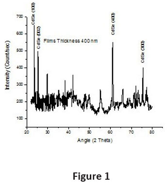 |
Figure 1 Click here to View figure |
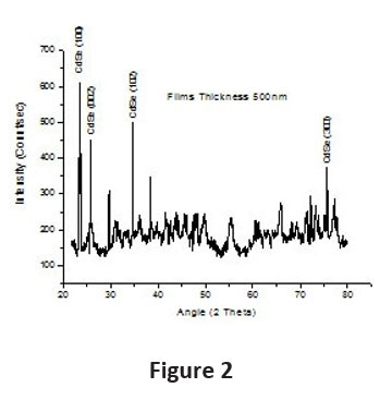 |
Figure 2 Click here to View figure |
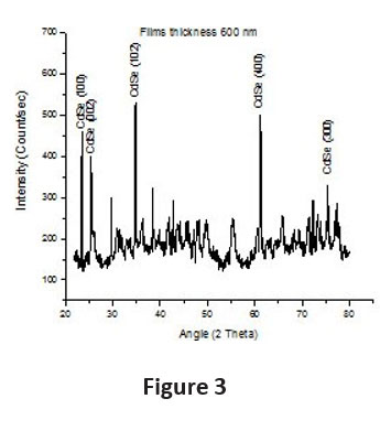 |
Figure 3 Click here to View figure |
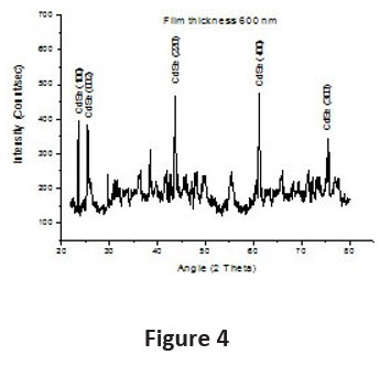 |
Figure 4 Click here to View figure |
From figures 5 to 7 it is clear that resistivity decreases with increase the film thickness and confirmed that films are semi-conducting nature because the resistivity decreases as increase in temperature. Hall Effect measurement confirmed that films are of n-type. Table-1 shows that carrier concentration increase with increase the film thickness.
Hall coefficient (RH ) = (VH X w) / (Ix . Bz) Carrier concentration (n) = 1/ ( RH . q ) Hall mobility (µH) = RH /
Where VH = Hall Voltage, Ix = Constant current in x- direction, Bz = Constant magnetic (400gauss) field in z- direction, = Resistivity of the film.
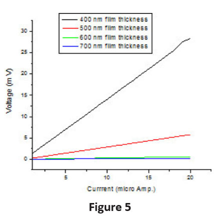 |
Figure 5 Click here to View figure |
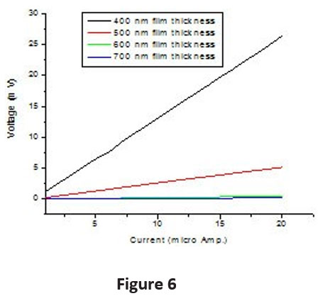 |
Figure 6 Click here to View figure |
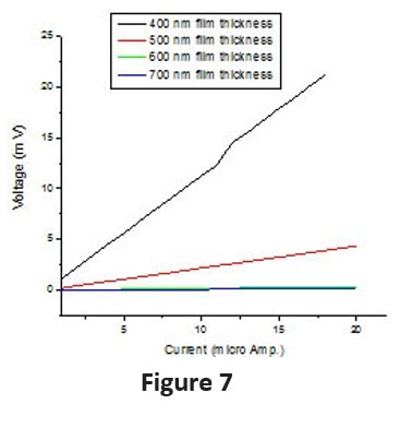 |
Figure 7 Click here to View figure |
Conclusions
In summary we concluded that the effect of films thickness on their electrical properties of the electron beam evaporated n-type CdSe thin films was investigated. The resistivity decrease from 321.245 × 10⁻³ to 3.4265 × 10⁻³ ohm-cm, charge concentration increases from 1.439 × 10¹⁷ to 19.75× 10¹⁷ per cm3 and also increases mobility from 135 to 923 cm2/volt sec with increases films thickness from 400 nm to 700 nm.
Acknowledgment
The authors wish to acknowledge the Department of Science and technology, government of India, New Delhi for providing financial support and also thanks for department of Nano Technology, Allahabad University, Allahabad for providing the facilities of XRD.
Conflict of Interest
There is no conflict of interest.
Funding Sources
There is no funding sources
References
- S.M. Hus and M. Parlak, Journal of Physics D. Appl. Phys. 41: 035405(8PP) (2008).
- K. Sarmah, R. Sarma, and H.L. Das, Journal of Physics Conference Series 114: 01204 (2008).
- K.D. Patel, R.K. Shah, D.L. Mukhija, V.M. Pathak, R. Srivastava- Journal of Ovonic research 4(6): 129-139 (2008).
- S.Erat, H. Metin, M. Ari- Material Chemistry and Physics 111: 114-120 (2008).
- O. Portillo-Moreno, R. Lozada-Morales, M. Rubin-Falfan, J.A. Parez-Alvarez, O. Zelaya- Angel, L. Banos-Lopez , Journal Phys. Chem. Solids 1751: 61 (2000).
- K. Bindu, M. Lakshmi , S. Bini, C. Sodha, Kartha, K.P. Vijaya, Kuma, T. Abe, Y. Kashiwada, Semi cond. Sci. Techol. 270: 17 (2002).
- T. Elango, S. Subramanian, R. K. Murali, Surf. coat. Technol. 8: 123 (2003).
- N.J. Suthan, Kissinger, M. Jayachandran, K. Peramal and C. Sanjeev Raja, Bull. Matter Sci. 30(6): 547-551 (2007). Indian Academy of Science
- Ralf Erni, Nigel D. Browing, Ultramicroscopy 107: 267-273 (2007).
- Sachin k. Sharma,Lakendra Kumar, Sushil Kumar, T.P. Sharma Chalcogenide letter 5(4): 73-78 (2008).
- D. Patidar, K.S. Rathore, N.S. Saxena, Kananbla Sharma, T.P. Sharma Chalcogenide letter 5(2): 21-25 (20
Accepted on: 12 Nov 2010


![]()
![]()
![]()
![]()