Depth Profiling of Aluminium Diffused in Silicon by Activation Analysis With 14 Mev Neutrons
1Department of Geology and Geophysics, I.I.T., Kharagpur - 721 302, India.
2Department of Physics, University of Poona, Pune - 411 007, India.
DOI : http://dx.doi.org/10.13005/msri/080225
Download this article as:
![]()
Here the technique of Activation analysis with 14MeV neutrons was used to know the depth profile of Aluminium in samples of p-type Silicon rubbed with Alumina and baked at high temperature(800oC). Chemical etching was done to remove layers and find the depth.
KEYWORDS:Semiconductors; Silicon; Aluminium; Depth profile; 14 MeV neutrons; Activation analysis.
Introduction
Diffusion of silicon with Aluminium is normally carried out to control electrical characteristics of silicon and also to manufacture semiconductor devices. It is known that different grain size alumina powders are used to polish crystalline silicon to meet experimental requirements. It may be possible that during polishing, aluminium atoms get diffused in silicon. However, so far no attention has been paid to study this diffusion and the depth profile of Aluminium in Silicon. The diffusion of aluminium in Silicon, at 800oC was analysed using 14 MeV neutron activation analysis.
Material and Methods
A silicon wafer (p-type) was rubbed for 2 hours with fine alumina powder (grain size in nanometers). The wafer was chemically cleaned and cut into pieces of dimensions 1cm2. Some of these samples were baked at 800oC in nitrogen atmosphere for a period of two hours.The Silicon sample rubbed with Alumina and the baked silicon samples rubbed with Alumina were exposed one by one to 14 MeV neutrons4-7 for an hour to induce the following nuclear reactions:
Al27(n,α)Na24
With t1/2=14.96 hours, Eg=1.369 MeV(100%), 2.73 MeV(100%) and
Si29(n,p)Al29
With t1/2=6.6 minutes, Eg=1.28 MeV(100%)
To avoid interference due to the gamma-ray emitted by other radioisotopes a cooling time of 30 minutes was given. The activity of energy 1.36 MeV was measured by a NaI(Tl) detector for 30 minutes was stored in the computer based MCA. Later on the silicon sample was etched in a HF solution, as the silicon wafer when stored for any length of time will often get covered by a top 50 Ao of oxide layer and this layer is removed using a short(about 40-60sec)etch consisting of HF:H2O::1:50 by volume whose etch rate is 70Ao / minute1 or can also be chemically polished in HF:HNO3::2:5(etch rate of 20µm).² By controlling the etch rate, 0.1µm surface layer³ of the silicon was removed. The activity of the Aluminium was then measured. This activity was subtracted from the earlier measured activity which gave the net activity due to aluminium atoms present in the first 0.1µm of the sample. After removing 0.1µm of the silicon layer each time the γ activity was measured and the experiment was repeated. Standard corrections for the half-life, background subtraction etc. were made and the results obtained.
Results and Discussion
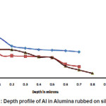
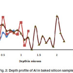
The results obtained from the activation analysis are shown in Figure 1 and 2. Figure 1 shows results for silicon samples which were mechanically rubbed with Alumina and activated to know the amount of aluminium in different layers after etching for three samples which were all irradiated for one hour. The results show Aluminium to be on the surface and less in the bulk. Figure 2 shows result for silicon samples which were not only rubbed with alumina but also baked at a high temperature in a oven kept at 800oC. Here the Aluminium has diffused from the surface to the bulk of the sample.
Figure 1: Depth profile of Al in Alumina rubbed on silicon
 Click on image to enlarge |
Figure 2: Depth profile of Al in baked silicon sample
 Click on image to enlarge |
Acknowledgements
I am grateful to the Council of Scientific and Industrial Research and Department of Science and Technology for their financial support
References
- Gandhi Sorab: “VLSI fabrication principles”, John-Wiley and sons
- Sarro P.M.:”Integrated silicon thermopile infrared detectors (Thesis)(1978)
- Katshui Yoshio et al., Japanese Journal of Phys., 21(5): L301 (1982)
CrossRef - V.N. Bhoraskar, Ind. J. Pure and Appl. Phys., 27: 648 (1989).
- L.F. Curtiss, An introduction to neutron physics, D. Van Nostrand Company, Inc., Princeton, New Jersey, (1959) .
- Technical report series no.273, Handbook on nuclear activation data by international atomic energy agency.
- C.M. Lederer, J.M. Hollander, and I. Perlman, Table of Isotopes, John Wiley and. Sons, New York (1967).
Accepted on: 28 Dec 2011


![]()
![]()
![]()
![]()