Niraj Kumar2, Anjana Kumari1, Manisha Samarth2, Rajiv Kumar2 And Tarun Kumar Dey2
1Department of Physics ,N.D College ,Purnea-854301, India.
2Department of Physics ,L.S College ,Muzaffarpur -842001, India.
DOI : http://dx.doi.org/10.13005/msri/110205
Article Publishing History
Article Received on : 14 Sep 2014
Article Accepted on : 29 Dec 2014
Article Published : 03 Nov 2014
Plagiarism Check: Yes
Article Metrics
ABSTRACT:
The current –voltage data of the metal –insulator semiconductor Schottky diode are simulated using thermionic emission diffusion equation taking into account the inter facial layer parameters.The computed current – voltage data are fitted into ideal thermionic emission diffusion equation to see the apparent effect of interfacial parameters on current transport.In presence of interfacial layer the Schottky contact behave as an ideal diode of apparently high barrier height. The behavior of apparent height and ideality factor with the presence of inter facial layer is discussed.
KEYWORDS:
Interfacial parameters: barrier height; ideality facto
Copy the following to cite this article:
Kumar N, Kumari A, Samarth M, Kumar R, Dey T. K. Analytical Studies of Metal Insulator Semiconductor Schottky Barrier Diodes. Mat.Sci.Res.India;11(2)
|
Copy the following to cite this URL:
Kumar N, Kumari A, Samarth M, Kumar R, Dey T. K. Analytical Studies of Metal Insulator Semiconductor Schottky Barrier Diodes. Mat.Sci.Res.India;11(2). Available from: http://www.materialsciencejournal.org/?p=681
|
INTRODUCTION
The metal–insulator–semiconductor (MIS) diode is the most useful device in the study of semiconductor surfaces. Since, the reliability and stability of all the semiconductor devices are intimately related to their surface conditions, an understanding of surface physics with the help of MIS diodes is of great importance to device operation [1–6]. The barrier height (BH) is an important parameter that determines the electrical characteristics of metal–semiconductor (MS) contacts. Schottky BH is defined as the difference in the energy between the metal Fermi level and band edge of the semiconductor majority carriers at the junction for a metal and semiconductor in contacts [1–3]. In general, being a Schottky contact configuration, its performance and reliability is drastically determined by the interface quality between the deposited metal and the semiconductor surface. It is well known that, unless specially fabricated, a Schottky barrier diode posses a thin interfacial native oxide layer between metal and semiconductor. The existence of such an insulating layer converts the MS device into a MIS device and has strong influence on its current–voltage (I–V) characteristics as well as the barrier parameters of Schottky diode [3,7] There are several possible reasons of error that cause deviation of the ideal behaviour of Schottky diodes with and without an interfacial insulator layer. These include the particular distribution of interface states [2,16], the series resistance [9,15,17], applied bias voltage [9,10,15,17,18] and device temperature [1,2,8–10]. In this paper, we analyse effect of an interfacial layer on I–V characteristics of Schottky diode using simulation studies.
BASIC THEORY
In the present paper, we consider a thermionic emission diffusion (TED) equation,the current through a Schottky diode as a function of applied voltage V is given by the expression [1–3]
where A is the diode area, A* the effective Richardson constant, q the electronic charge, k Boltzmann constant, T the absolute temperature, fb the BH at zero bias, Z is the ideality factor which is measure of conformity of the diode behaviour to pure thermionic emission theory and is a dimensionless factor introduced to account for deviation from TED theory. The deviation from pure thermionic emission may arise due to the presence of an interfacial insulator layer between metal and semiconductor, surface charges and image force effects. For a Schottky diode with an interfacial insulator layer, Card and Rhoderick [2] reported that the relation between the applied bias V and current I is same as Eq. (1), with an additional exponential factor dependent on interfacial layer parameter as given by
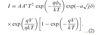
The factor (a√ϰδ) is known as the electron tunneling factor, a = (4π / h) (2m*)1/2 is a constant, m* = 0.067 m0 the effective tunneling mass of electron, m0 is the rest mass of electron, k is the mean tunneling barrier presented by thin inter facial layer which is expressed as energy difference between the conduction band edge of the semiconductor and that of the inter facial layer, is the thickness of an inter facial insulator layer.
The Eq. (2) is similar to standard thermionic emission equation for Schottky diodes with except for the factor exp (-a√ϰδ) which is the tunneling probability and is characteristics of inter facial layer. Occurrence of exponential factor in the current equation yields the I–V curves of diode same as that of a diode without an interfacial layer but shift the starting point of the I–V curves towards low current which corresponds to decreased value of the saturation current and in turn give rise to high apparent BH. This apparent BHΦap , at temperature T, with an inter facial insulator layer of thickness is given by
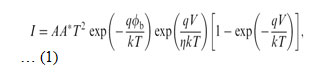
If an inter facial layer is extremely thin, then (-a√ϰδ) is unity and BH of the diode remains unaltered by its presence. In the usual analysis of the experimental or simulated data of Schottky diode with an inter facial layer using Eq. (2), the apparent BH and idea lity factor a redetermined form the extrapolated current at zero bias and slope of the linear region of lnI–V curve, respectively,using fitting of I–V data into Eq. (1). The apparent BH and ideality factor thus obtained, when analysed as a function of temperature reflects the effect of an inter facial layer on Schottky diode behaviour. Simulation of the I–V data of Schottky diodes with the presence of an inter facial layer between the metal and semiconductor has been performed by calculating the total current applying Newton–Raphson iteration method using Eq. (2). The I–V data thus obtained is fitted into ideal TEDEq. (1) to see the apparent effect of an inter facial layer on the behaviour of diode parameters such as BH, idea lity factor and series resistance.
RESULTS AND DISCUSSION
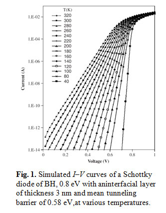
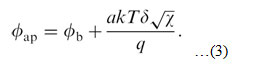
Simulation of I–V data of Schottky diode with an inter facial layer is performed for the Schottky diode areaA = 7.87 × 10⁻⁷ m-2, corresponding to a 1 mm diameter metal dot, effective Richardson constant A* = 1.12× 10⁶ Am-2 K-2 (for n-type silicon) and = 0.8V. An interfacial layer parameters taken for simulation of I–Vdata are = 0.58 eV and = 3 nm. These are typical values reported in the literature for experimentally fabricated MIS contacts [7,9,19,21]. The ln(I)–V plots thus obtained at various temperature are shown in Fig. 1. From Fig. 1 it is clear that behaviour of ln(I)–V curves is almost same as that of a Schottky diode without an inter facial layer [20]. These curves are linear over several orders of current at lower temperatures. To see the effect of an inter facial layer on barrier parameters the I–V data shown in Fig. 1 are
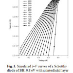 |
Fig1: Simulated I–V curves of a Schottky diode of BH, 0.8 eV with an inter facial layer of thickness 3 nm and mean tunneling barrier of 0.58 eV,at various temperatures.
Click here to View Figure
|
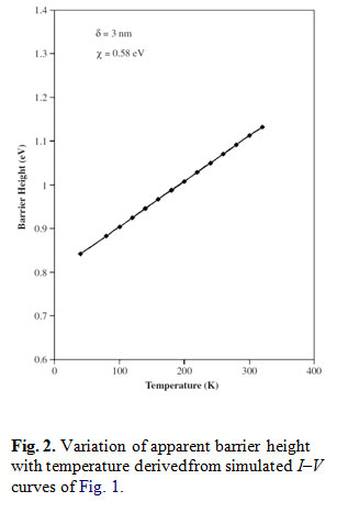
fitted into Eq. (1) using least square method to derive apparent BH, ideality factor and series resistance. Fig. 2shows the apparent BH obtained from the simulated dataat various temperatures. It is evident from Fig. 3that the apparent BH of Schottky diode with an interfacial layer increases above the value of BH of pure MS contact.However, the ideality factor of the diodes, not shown here,remains unity at all temperatures. As shown in Fig. 4 the apparent BH of MIS Schottky diode decreases linearly with fitted into Eq. (1) using least square method to derive apparent BH, ideality factor and series resistance. Fig. 2shows the apparent BH obtained from the simulated dataat various temperatures. It is evident from Fig. 3that the apparent BH of Schottky diode with an interfacial layer increases above the value of BH of pure MS contact.However, the ideality factor of the diodes, not shown here,remains unity at all temperatures. As shown in Fig. 4 the apparent BH of MIS Schottky diode decreases linearly with
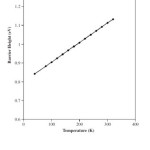 |
Fig2: Variation of apparent barrier height with temperature derived from simulated I–V curves of Fig. 1.
Click here to View Figure
|
inter facial insulator layer yields increased apparent BH, which decreases linearly with decrease in temperature, while the ideality factor of the diode remains unity.
The interesting observation here is that presence of an inter facial layer makes BH increase from its value (0.8 eV,here) that exists for a pure intimate MS contact without an inter facial layer. At any temperature the BH increases by an amount (aKtδ√ϰ/q) and obviously depends linearly on temperature. The increase in value of apparent BH of MIS contact is more at room temperature and it approaches value of pure MS contact at 0k. This behaviour of apparent BH with decreasing T is slightly different from the observed behaviour of experimentally fabricated MIS contacts [9,13,22,23]. In this paper, the apparent BH is shown to decrease linearly with decrease in temperature but the overall BH remains lower than BH of corresponding MS contact. The similarity in the results reported from experimental work and in our calculation is that BH decreases linearly with decrease in temperature. However,the experimentally observed BH values varies over low BH range than those shown in Fig. 2 obtained by numerical simulation using the proposed theory of current conduction in Schottky diodes with an inter facial layer [7,9,22–27].Similar linear decrease of BH with decreasing temperature is also reported for Schottky diodes with inversely doped surface layer and the apparent BH is smaller than the BH considered for pure MS system [28].
There are other reports on current transport studies of Schottky diodes with an inter facial layer [7,19]. The variation of BH as a function of T reported in these studies is non-linear and is in consistent with the current transport theory of a Schottky contacts with an inter facial layer [7,22–26]. The results reported on Schottky contacts with intentionally grown inter facial layer shows very small increase in BH of MIS diode as compared to the measured BH of pure Schottky diode without an inter facial layer[20,21]. These experimental observations on high BH of Schottky diode with an inter facial layer are consistent with Eq. (3).
The I–V data of Schottky diodes with different inter facial layer thickness and mean tunneling barrier were generated. The behaviour of the ln(I)–V plots for different thickness and mean tunneling barrier is almost the same. The apparent BH increases with increasing interfacial layer thickness and mean tunneling barrier. The current depends on the tunneling probability exp (-a√ϰδ) through an inter facial layer, because of which the current decrease with increasing inter facial layer thickness or mean tunneling barrier and subsequently, the apparent BH increases. Figs. 3 and 4 shows the apparent BH as obtained from the simulated curves at different temperatures for various values of inter facial layer thickness and effective mean tunneling BH, respectively. From these figures, it isevident that increase in mean tunneling barrier or an inter facial layer thickness makes the apparent BH increase.
It is obvious from the results obtained from the simulated I–V data of a Schottky diode with an inter facial layer that the value of ideality factor remain unity at all temperatures. However, the experimental data reported inthe literature yields ln(I)–V plots having greater than unity ideality factor [19,22, 23,24]. More over, the reported ideality factor is temperature dependent. In order to havegreater than unity ideality factor from the simulated current–voltage data, we undertake the following analysis.
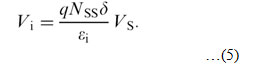
It is well established that BH is considered to be bias dependent, which give rise to high ideality factor in Schottky diodes [1,2]. In case of MIS contact mean tunneling BH,k is a similar parameter which governs the current transport across the diode according to Eq. (2). Asthe BH varies with applied bias, correspondingly the mean tunneling barrier should also be a function of bias.Therefore, we assume bias dependence of mean tunneling barrier and generate the ln(I)–V plots of the MIS contact.Fig. 5 shows the ln(I)–V plots of MIS contacts with and without bias dependence of mean tunneling barrier k .
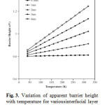 |
Fig3: Variation of apparent barrier height with temperature for various inter facial layer thicknesses and mean tunneling barrier of 0.58 eV.
Click here to View Figure
|
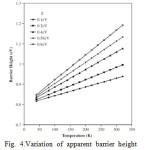 |
Fig4: Variation of apparent barrier height with temperature for various mean tunneling barrier and inter facial layer thickness of 3 nm.
Click here to View Figure
|
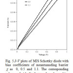 |
Fig5: I–V plots of MIS Schottky diode with bias coefficients of mean tunneling barrier k as 0, 0.5 and 1.1. The corresponding values of ideality factor for these bias coefficients are 1, 1.12 and 1.28, respectively.
Click here to View Figure
|
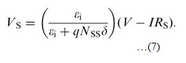
It is clear from Fig. 5 that ln(I)–V plots with bias dependent exhibit ideal shapes with less slopes and hence high ideality factor. The least square fitting programme is used to extract BH, Z and RS. From the ln (I)–V curves with bias dependence of k, it is observed that the value of BH and RS remains same as obtained from the curves without considering bias dependence of k. The derived ideality factor as a function of temperature is shown in Fig. 6. It is clear from Fig. 6 that the bias dependence of k gives rise to high idea lity factor. However, the ideality factor decreases with decreasing temperatures. The experimental results reported in literature shows that ideality factor of MIS diodes increases with decreasing temperature, whereas theI–V data obtained by simulation using bias dependence k of yields linearly decreasing ideality factor with decreasing temperature. Thus, the simulation result shows that the bias dependence of tunneling BH cannot account for high idea lity factor of MIS Schottky diode and consequently the temperature dependence of ideality factor.
Potential drop across an inter facial layer is another cause widely cited in the literature, which is believed to give rise to high idea lity factor in MIS diodes [3,5,9,23,24]. We further simulated the I–V data of a MIS diode taking into account potential drop across an inter facial layer. The drop across an inter facial layer is modeled during numerical simulation for generating I–V data of a MIS diode using Eq. (2). The forward voltage V applied across the device partially appears across the series resistance as IRS, Vi across an inter facial layer and VS across the device/diode and can be expressed as [23,24]
V = Vs + Vi +IRS…….(4)
The voltage across an inter facial layer Vi is given by [23]
From Eqs. (4) and (5), the voltage across an interfacial layer is given by
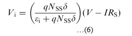
and the actual voltage that appears across the diode which governs current flow through it, is given as
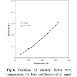 |
Fig6: Variation of ideality factor with temperature for bias coefficient of k equal to 1.1. It depicts that the ideality factor decreases almost linearly with decreasing temperature.
Click here to View Figure
|
Thus, considering potential drop across an inter facial layer, the voltage that actually appears across the device is less than the applied bias as given by Eq. (7). Clearly this voltage is function of inter facial layer thickness ‘δ’,interface state density ‘Nss’ and inter facial layer permittivity ξi. The ln(I)–V plots of MIS contact are simulated taking into account the voltage drop across an inter facial layer.The ln(I)–V plots (not shown here), obtained by considering voltage drop across an inter facial layer exhibits lesser slope and thus correspond to high ideality factor. The ln(I)–V plots are generated at various temperatures and ideality factor was estimated by fitting of simulated data into Eq. (1) at all temperatures. The interesting observation is that the ideality factor increase above unity depending on the values of , and Nss and attains same value at all temperatures. As an example for ξi = δ Nss and attains same value at all temperatures. As an example for ξi = 7 x ξσ, δ = 3 and Nss= 4.0 ×10¹⁶ eV-1 cm-2, ideality factor attain value 1.30 at all temperature. It is obvious from Eq. (7) that the ideality factor is reciprocal of the factor (εi | ( εi + a Nss)), which gives rise to voltage drop across an inter facial layer.Since, this factor does not contain temperature term there fore ideality factor remains same when I–V data is calculated at various temperatures. As the ideality factor is believed to be arising due to the voltage drop across an inter facial layer, it will exhibit temperature dependence only if any of the factor in this expression is temperature dependent. We have investigated this expression and are of the opinion that the parameter, which can be temperature dependent is the interface state density ‘Nss’. So far, in simulating I–V data ‘Nss’ is assumed to have constant value and thus ideality factor remains constant at all temperatures.For ideality factor to vary with temperature the inter face state density must exhibit temperature dependence.Like the density of states in energy bands in solid has T3/2 dependence, we assume same temperature dependence of interface state density ‘Nss’. The I–V data of MIS Schottky diode thus generated at various temperatures yield η decreasing with lowering temperature. In order to have high η at low temperatures Nss should exhibit inverse temperature dependence. Thus, we assume in verse temperature dependence of ‘Nss’ and simulated ln(I)–Vplots for different exponents of T.Fig. 7 shows variation inZ as a function of temperature for various exponent of T.Interestingly, the observed increase in ideality factor with decreasing temperature is almost identical to reported variation of ideality factor obtained from the experimental data on MIS contacts [12,13]. Thus, increase in ideality factor with decreasing temperature is only possible if the inter face state density is assumed to have inverse temperature dependence.
 |
Fig7: Variation of ideality factor of MIS Schottky diodes with temperature. Note different rising trend of ideality factors for different temperature dependence of interface state density.
Click here to View Figure
|
Inverse temperature dependence implies that more inter face states are effective at low temperature.It can be further related to the available energy levels of inter face states. At higher energies there is less density of states, while at low energies more states are available.Thus, more energy levels of interface states will be at low energies. At low temperature electron transport may occur through deep level, traps/states, where as at high temperature due to high energies of electrons, shallow traps/states may participate in conduction process at the interface.Therefore, at low temperature electron transport occur via deep traps/states, which are more, so effective density of states is more and hence the resulting ideality factor arising due to potential drop across the layer increases. On the other hand, at high temperature electron transport may occur via shallow traps/states, which are less in number,thus leading to relatively low ideality factor. The similar inverse temperature dependence of interface state density derived from the experimental work on MIS Schottky diodes is also reported in the literature [7,9,13,28]. The actual temperature dependence of interface state density at the MIS junction will governs the rising trend of ideality factor with decreasing temperature. Exact distribution of inter face state density will shed more light on under standing the behaviour of MIS Schottky diodes, which requires more investigation and is open for future discussion.
CONCLUDING REMARKS
The I–V characteristics of Schottky diodes with an inter facial insulator layer are studied by numerical simulation.The I–V data of the MIS Schottky diode are generated using TED equation considering an interfacial layer parameters. The calculated I–V data are fitted into ideal TED equation to see the apparent effect of an inter facial layer on barrier parameters. It is shown that mere presence of an inter facial layer at the MS inter face makes Schottky diode behave as an ideal diode of high apparent BH. The apparent BH is shown to decrease linearly with decreasing the temperature. However, the ideality factor and series resistance remains same as considered for a pure Schottky contact without an inter facial layer. It is shown that bias coefficient of mean tunneling barrier, however, increases the ideality factor, but makes ideality factor decrease with decreasing temperature.Considering the potential drop across an inter facial layer also give rise to high ideality factor, which remains constant at all temperatures. The inverse temperature dependence of interface states is suggested to be the possible reason for causing increase in ideality factor with decreasing device temperature.
REFERENCES
- RhoderickE.H., Williams,R.H. Metal–Semiconductor Contacts,Clarendon, Oxford,(1988).
- Card,H.C. Rhoderick,E.H. J. Phys. D 4 1589(1971).
CrossRef
- Yalcin,A. Turut,Saglam, N. M. Solid State Electron. 35 835(1992).
- Cowley,A.M. Sze,S.M. J. Appl. Phys. 36 3212(1965).
CrossRef
- Tseng,H.H. Wu, C.Y. Solid State Electron. 30 383, (1987).
CrossRef
- Hudait,M.K. Kruppanidhi,S.B. Solid State Electron. 44 1089(2000).
CrossRef
- Altindal,S. S. Karadeniz, N. Tugluoglu, A. Tataroglu, Solid StateElectron. 47 1847(2003).
CrossRef
- Dokme I, Altindal S, Semicond. Sci. Technol. 21 , 1053,(2006) .
CrossRef
- WernerJ.H., Appl. Phys. A 47 291(1988).
CrossRef
- Hardikar S, HudaitM.K, ModakP, KrupanidhiS.B., PadhaN.,Appl. Phys. A 68 , 49.(1999)
CrossRef
- Tugluoglu N, Karadeniz S, Altindal S, Appl. Surf. Sci. 239 ,481.(2005)
CrossRef
- Karatas S, Altindal S, Solid State Electron. 49 , 1052,(2005).
CrossRef
- Karatas S, Altindal S, Mater. Sci. Eng. B 122, 133,(2005).
CrossRef
- Temircl C, Bati B, Saglam M, Turut A, Appl. Surf. Sci. 172 (2001) .
- Biber M, ,Turut A, Electron. Mater J,.31 , 1362,(2002).
CrossRef
- Cetin H, Sahin B, Ayyildiz E, Turut A, Physica B 364 133,(2005) .
CrossRef
- Akkilic K, Kilicoglu T, Turut A, Physica B 337 , 388 (2003).
CrossRef
- Osvald J, HorvathZs.J., Appl. Surf. Sci. 234 , 349 (2004).
CrossRef
- Yadaiah et al.Mat . Sci.Res. India.6(2) 263-278(2009).
CrossRef
- Biber M, Physica B 325, 138(2003).
CrossRef
- Aydin M.E, Akkilic K, T. Kilicoglu, Appl. Surf. Sci. 225 , 318 (2004).
CrossRef
- Biber M, Coskun C, Turut A, Eur. Phys. 31 , 79(2005).
- Aydin M.E, Akkilic K, Kilicoglu T, Physica B 352 , 312 (2004).
CrossRef
- Altindal S, Dokme I, Bulbul M.M, . Yalcin N, Serin T, Microelectron.Eng. 83, 499(2006).
CrossRef
- Rafferty. C.S., Pinto. M. R., and Dutton. R. W. ‘Semiconductor device modeling’, IEEE, Elec. Dev. vol. ED-32, , pp- 2018-2027 (2010).
- DeyT.K, Kumar R and Kumari A,J.PAS 17,203-211 (2011)

This work is licensed under a Creative Commons Attribution 4.0 International License.