Khalil El-Hami1, Cristina Louro2 and Albano Cavaleiro2
1Univ. Hassan, Faculty of Khouribga, Laboratory of Nanosciences and Modeling,PB:145,Khouribga City, MOROCCO
2Univ. Coimbra, SEG-CEMUC, Center of Mechanical Engineering, Polo II, 3030-788, Coimbra city, PORTUGAL
DOI : http://dx.doi.org/10.13005/msri/110202
Article Publishing History
Article Received on : 31 Oct 2014
Article Accepted on : 10 Nov 2014
Article Published : 01 Dec 2014
Plagiarism Check: Yes
Article Metrics
ABSTRACT:
The tungsten disulfide (WS2) thin films, considered as inert, non-toxic, non-corrosive lubrication that is resistant to most fuel solvents, is the best solid lubricant for general industry. In this paper, WS2 thin films were deposited on steel and silicon <110> type substrates by DC sputtering methods with optimized experimental conditions and parameters. Scanning Electron Microscopy (SEM) and Atomic Force Microscopy (AFM) were employed to characterize the surface morphology and determine the geometrical size of WS2 lamellae or microtubes. The investigation showed that both SEM and AFM analysis revealed oriented WS2 crystalline lamellae on silicon substrate while they are entangled on the steel substrate. This result leads to say precociously that the WS2 thin films deposition depend on the substrate type. Moreover, using the AFM results, we could determine the average lamella (or microtube) size which has from 200 nm to 500 nm in width and from 1mm to 1.5mm in length. The EDS tool allows attaining the composition of deposited WS2 where the tungsten and the disulfide represent about 40 and 55%, respectively.
KEYWORDS:
Tungsten disulfide; Scanning Electron Microscopy; Atomic Force Microscopy; EDS; WS2 lamellae; texture orientations
Copy the following to cite this article:
El-Hami K, Louro C, Cavaleiro A. Sized WS2 Lamellae and their Texture Orientations Growth. Mat.Sci.Res.India;11(2)
|
Introduction
The application of thin films for tribological and mechanical devices has attracted considerable interest in the recent past [1] Especially; the tungsten disulfide (WS2) has been largely studied and characterized for various applications [2-8].
The main application of the WS2 is used for solid film lubricant. Physical vapor deposition (PVD) is a widely used technique of depositing thin films by sputtering, that is ejecting, material from a target, that is source, which then deposits onto a substrate [9] . Sputtered atoms or ions ejected from the target have a wide energy distribution, at higher gas pressures, they collide with the gas atoms that act as a moderator and move diffusively, reaching the substrates or vacuum chamber wall and condensing after undergoing a random walk. The sputtering gas is often an inert gas such as argon. Sputtering is used extensively in the semiconductor industry to deposit thin films of various materials in integrated circuit processing. Thin antireflection coatings on glass for optical applications are also deposited by sputtering [10].
Experimental Setup
Tungsten disulfide WS2 thin films were deposited on steel and silicon <110> type substrates by DC sputtering methods. We chose rotating than fixed substrates, in the sputtering chamber, in order to reduce the coefficient of friction and wear and obtain a long wear life of the film. On the other hand, rotating substrates have economic impact by using lot of samples. The efficiency of the solid film lubricant depends on the degree of adherence of the film to the surface to be lubricated. For this reason, the surface pretreatment with argon in ultra-high vacuum, the energetic of the sputtered material using approximately 700 V, the type of the substrate materials and type of interface for med play a key role for the adherence process and determines the durability and wear of the sliding components.
Results and Discussion
Optical Microscope Characterization
From optical microscope image (Fig.1) we can see a large area of the deposited WS2 film showing homogenous and uniform film without holes or roughness in Fig.(a), and the standing WS2 lamellae as rod-like in Fig.(b). This result was due to many experiments on DC sputtering methods to optimize all parameters and conditions such as value and time of applying voltage, argon ratio, etching condition, distance between target and substrate and so on.
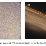 |
Fig1: Optical microscope image of WS2 on Si substrate, (a) on the top, (b) at the edge (100x100mm).
Click here to View figure
|
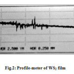
Profile-Meter Determination
To determine the thickness of the deposited of WS2 film, we used a profile-meter technique. A step, suitable for surface profiling, was provoked on the film edge by using boron nitride and then acetone. The detection of the scanned edge gives the projected wall thickness. The profile-meter indicates a WS2 film thickness of about 2.5 mm as shown in Fig.2. We notice the presence of significant drift.
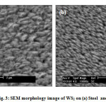
SEM Characterization
The SEM images in Fig. 3 reveal oriented WS2 crystalline lamellae on Si substrate than on the steel substrate. At first study, we can suggest that the structure of WS2 lamellae took a preferential orientation on Si <110> substrate while they were entangled on the steel substrate.
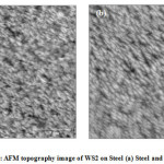
AFM Characterization
The tapping mode AFM is used to obtain topography images of WS2 thin film on both steel and Si substrates. The conditions of the tapping mode used in this investigation with a tip of silicon doped under the frequency of 373 KHz, stiffness of 30 N/m and a speed of 0.5 Hz.
The AFM topography images showed the same observation as in SEM in which WS2 crystalline lamellae are oriented on Si substrate in a preferred direction than on steel substrate. We notice that we used a Si wafer <110> and the WS2 lamellae are following these directions. The suggestion may lead to say precociously that the film deposition depends on the substrate.
Characterization of WS2 Lamellae
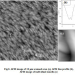 |
Fig5: AFM image of 10 mm scanned area (a), AFM line profile (b), AFM image of individual lamella (c)
Click here to View figure
|
Referring to the Fig.5, the AFM image shows homogeneous and uniform thin film of WS2 containing crystalline lamellae texture. The geometry of individual lamella is sized from 200 nm to 500 nm in width and from 1mm to 1.5 mm in length.
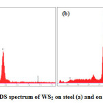
EDS characterization
The characterization of WS2 on steel substrate by EDS is shown in the spectrum of the Fig. 6. As we can see, the tungsten (W) and sulfide (S) represent, respectively, ratio of 40,83% and 53,39%. The approximately ratios of W and S were found on the Si substrate (Wratio = 41,04% and Sratio = 53,15%).
Conclusions
The investigation on sputtered tungsten disulfide (WS2) thin films showed different textures of crystalline lamellae deposited on steel and silicon substrates. These preferred orientations influence and will have effect on tribological properties of WS2. Further experimentations concerning the growth of WS2 on different surfaces like KBr, NaCl or highly ordered pyrolytic graphite (HOPG) substrates could be interesting and will be a widespread topic of the coming investigations.
Acknowledgements
The authors wish to thank the Erasmus Mundus Al-Idrisi for funding the research reported under the Grant Agreement number 2011-2480-001-EMA2. The first author, also, would like to thank SEG-CEMUC for using their instruments for experiments.
References
- C.D. Dimitrakopoulos, P.R.L. Malenfant, Adv. Mater. 14 (2002) 99.
CrossRef
- G. Seifert, H. Terrones, M. Terrones, G. Jungnickel, T. Frauenheim, Solid State Commun. 114 (2000) 245.
CrossRef
- G. Seifert, H. Terrones, M. Terrones, G. Jungnickel, T. Frauenheim, Phys. Rev. Lett. 85 (2000) 146.
CrossRef
- L. Scheffer, R. Rosentsveig, A. Margolin, R. Popovitz-Biro, G. Seifert, S.R. Cohen, R. Tenne, Phys. Chem. Chem. Phys. 4 (2002) 2095.
CrossRef
- M. Remskar et al., Science 292 (2001) 479.
CrossRef
- R.L.D. Whitby et al., Chem. Mater. 14 (2002) 2209.
CrossRef
- R.L.D. Whitby, W.K. Hsu, C.B. Boothroyd, H.W. Kroto, D.R.M. Walton, Chem. Phys. Lett. 359 (2002) 121.
CrossRef
- L. Rapoport, Y. Bilik, Y. Feldman, M. Homyonfer, S.R. Cohen, R. Tenne, Nature 387 (1997) 791.].
CrossRef
- Vasilyeva, E.S.; Tolochiko, O.V.; Kim, B.K.; Lee, D.W.; and Kim, D.S.; “Synthesis of Tungsten Disulfide Nanoparticles by the Chemical Vapor Condensation Method;” 2008.
- Rosentsveig, R.; Morgolin, A.; Feldman, Y.; Popovitz-Biro, R.; and Tenne, R.; “WS2 Nanotube Bundles and Foils; Chem, Mater.14; 2002.

This work is licensed under a Creative Commons Attribution 4.0 International License.