Electrochemically Developed Micro/Nanostructures in Single Ion Track Filters As a New Pattern
S. Amrita Kaur*
Department of Physics Khalsa College, Amritsar,143001.
Corresponding Author Email address: sanjitamrita@gmail.com
DOI : http://dx.doi.org/10.13005/msri/120109
Article Publishing History
Article Received on : 12 Jun 2015
Article Accepted on : 25 Jun 2015
Article Published : 25 Jun 2015
Plagiarism Check: Yes
Article Metrics
ABSTRACT:
The technique of pattern synthesis using potentiostatic electroless deposition is a very weighty process for fabrication of micro/nano structures and is cheap and simple. In this paper, electrochemical/electroless deposition have been used to develop copper micro/nanostructures within the micro/nanochannels of single ion track membranes. Scanning electron microscope was used for morphological studies. These micro/nanostructures have uniform diameters of 5µm and 200nm which is equivalent to the pore shape and size of the pattern used.
KEYWORDS:
ion track filters; pattern; electroless deposition; nanostructures
Copy the following to cite this article:
Kaur S. A. Electrochemically Developed Micro/Nanostructures in Single Ion Track Filters As a New Pattern. Mat.Sci.Res.India;12(1)
|
Copy the following to cite this URL:
Kaur S. A. Electrochemically Developed Micro/Nanostructures in Single Ion Track Filters As a New Pattern. Mat.Sci.Res.India;12(1). Available from: http://www.materialsciencejournal.org/?p=2533
|
Introduction
The micro/nanoscale materials have been used to developed many sophisticated devices now a days. Some desired materials can be deposited using ion track filters (ITFs) as a pattern for the fabrication of micro/nanostructures. These structures find immense applications in the area of materials science, nanoelectronics, magnetic devices, chemical and biological devices [1-5]. There are many procedures used in the production of nanowires, but template synthesis is elegant, adaptable and cheap for fabricating the variety of nanomaterials including metals, semiconductors, conducting polymers etc.[6-10]. Development of micro/nanostructures comprising either metallic or semiconductor dots, fibres, wires, cones, tubules or whiskers have provided exciting applications in multidisciplinary fields[6,11]. Another use of these microstructures containing hollow tubules lies in fabrication of volcano field ion sources and field emission of copper nano wires[12,13] . Synthesis of polymeric micro/nano capsules arrays have been used for field emission properties [14] and enzyme immobilization,[15] bio/chemical sensors, a large number of industries will benefit from the high tech track etched polymer membranes [16,17] , such structures may be used in magnetic data storage devices[18], superconducting wires[19] ph-sensors [6] etc. It has been observed that ITFs based pattern synthesis have gained weightage due to their nanoscopic dimensions which creates an inquisitive nature for the micro/nano structural understanding, properties and their potential use for different technological applications. In this research work, copper micro/nanostructures were developed from polymeric ion track filters (ITFs).
Materials and Methods
The pattern synthesis technique help us to deposit a suitable metal ions within the pores of the filters electrochemically for the generation of various structures viz. shorts, squat fibrils, tubules, rods, wires etc. These generated geometries depend upon the pore size and shape of the ITFs with complete control over the aspect ratio (length to diameter ratio). The metal rods were obtained by chemically depositing metal preferentially on the pore walls. In the present work, samples of various polymer films were irradiated by different heavy ion beams. All the samples were irradiated at an angle of 90o with respect to the surface of the films. The irradiated samples were etched in different solutions at different temperatures, 40, 50, 60 and 70°C. The etched samples were soaked in the folds of a tissue paper. Here, we have used the simple method of electroless deposition of metal into the etched pores of polymeric ITFs by using a self designed cell. The suitable electrolyte was made in high resistivity ion-free water. After the completion of electroless deposition, the electrolyte was drained out and the copper electrode was detached from the copper substrate. After drying, the ITFs were removed by dissolving it in an appropriate chemical, followed by rinsing with water and ethanol. The gold sputtering is done on produced micro/nanostructures and then scanned under scanning electron microscope (SEM) for studying its morphology and structure details.
Experiments and Results
Production of ion track pores in polymer
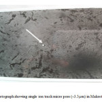
In particular, polycarbonate membranes (Makrofol-KG) of thickness 30µm and 10µm, irradiated with heavy ion 132Xe of energy 14.5 MeV/u and U238 of energy 14.0 MeV/u having fluence 105 & 108 ions/cm2 at normal incidence from UNILAC accelerator, GSI, Darmstadt, Germany. These samples were chemically etched at temperature 400C and 200C, for 30 and10 minutes, respectively in etchant 6.25 N NaOH solution. The pores obtained are cylindrical having pore diameter of size 3.5µm and 200 nm and vary linearly with etching time.
Figure1: Photograph showing single ion track micro pore (~3.5µm) in Makrofol-KG.
Production of copper micro/nano rods:
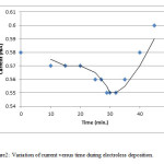
A thick copper tape was applied to one side of the ion track filters (ITF) as cathode and pure copper wire as anode in the self designed cell. The electrolyte was made up of an aqueous solution of 0.2 g/ml CuSO4.5H2O and 0.025 g/ml dil. H2SO4. Electroless deposition was performed potentiostatically at room temperature i.e 38±1°C using ITFs. Fig.2 shows the graph of current versus time during electroless deposition process.
Figure2: Variation of current versus time during electroless deposition.
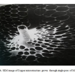
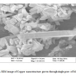
The Copper nanorods generated after using ITFs as pattern were immediately removed from the electrolyte after the electroless deposition process was over, which was then followed by washing with distilled water and ethanol and finally dried in air at room temperature. After drying, the polymer in the micro/nanostructure was removed by dissolving it in chloroform for 5 minutes for further analysis. The cleaned and dried samples were mounted on aluminium stubs using double adhesive tape. The gold palladium alloy sputtering was done and viewed under “Carl Zeiss Supra 55 Scanning Electron Microscope” at an accelerating voltage of 10 KV. The micro and nanostructures of copper (Cu) grown through the single-pore ITFs of Makrofol-KG are shown in Figures 3 and 4, respectively. Figure 5 shows the enlarged view of a single nanostructure.
Figure3: A SEM image of Copper microstructure grown through single-pore of Makrofol-KG.
Figure4: A SEM image of Copper nanostructure grown through single-pore of Makrofol-KG.
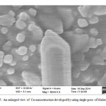
Figure5: An enlarged view of Cu-nanostructure developed by using single-pore of Makrofol-KG.
Discussion
The ITFs have advantages for their use as pattern for the fabrication of micro/nanostructures due to their well defined pore size over other membranes like alumina, glass membranes, zeolites etc. The porosity, pore diameter and pore length of these filters can be controlled by ion characteristics and etching parameters like etching time, etching temperature and etchant concentration. The morphological study of these structures developed from etched tracks in polymer films as a pattern, provided a fine and critical geometry and dimensions of micro/nano structure. It also empowers to study the various aspects of interaction of a heavy ions with given material leading to formation of ITFs. The metallic structures also reveal detailed components of etched pores i.e. diameter, length, shapes. These studies are further helpful for analysis of track profiles and applications in micro and nanotechnology.
Conclusion
These produced copper structures in nanoscale range by using ITFs plays an important role for the advanced studies of basic science and various applications in diverse area. It provides us the simplest route to nanotechnology and generation of nanodevices. The nanorods have high ability for their use as field emission studies, magnetic storage and recording devices, sensors etc.
Acknowledgements
The author is highly obliged to Dr. Reimer Spohr of GSI, Darmstadt, Germany for providing irradiation facilities and also grateful to Prof. H. S. Virk and Prof. S. K. Chakarvarti for providing me the valuable guidance and Dr. Jaskiran Kaur, Department of Physics G.N.D.U. Amritsar for providing me the SEM facilities.
References
- Perry J.L., Guo P., Johnson S.K., Mukaibo H., Stewart J.D. and Martin C. R., Nanomedicine, 5 1151-1160 (2010).
CrossRef
- Bhatt M. P., Magurudeniya H.D., Rainbolt E. A., Huang P., Dissanayake D.S., Biewer M.C. and Stefan M.C., J. Nanosci. And Nanotechnol. 14 2, 1033-50 (2013).
CrossRef
- Hiruma K., Yazawa M., Katswyama T., Ogawa K., Haraguchi K. and Koguchi M., J. of Appl. Phys., 77, 447-462 (1995).
CrossRef
- Klein J.D., Herrick R.D., Palmer D. and Sailor M.J., Chem. Mater. 5, 902 (1993).
CrossRef
- Fleischer R.L., Price P.B. & Walker R.M., Nuclear tracks in solids: Principles and Applications, University of California press, Berkely, (1975).
- Martin C.R., Science, 266, 1961(1994).
CrossRef
- Chakarvarti S.K., Ind. J. Phys. 83 6, 737-749 (2009).
CrossRef
- Fink D., Alegaonkar P.S., Petrov A.V., Withelm M., Szimkowiak P., Behar M., Sinha D., Fahrner W.R., Hoppe K. and Chadderton ,L.T., Nucl. Intr. Methods in Physics Research B, 236, 11-20 (2005).
CrossRef
- Penna D.J., Mbindyo J.K., Carado A.J.,Mallouk, T.E., Keating C.D., Razavi B. and Mayer T.S., J. Phys. Chem. B106, 7458 (2002).
CrossRef
- Iwasaki T., Motoi T. and Den T., Appl. Phys. Lett. 75, 2044 (1999).
CrossRef
- Mikailzade F. and Aktas B., Nanostructured materials for magnetoelectronics, Springer Verlag, Heidelberg, Germany, (2013).
- Fischer B.E. and Spohr R. Rev. Mod. Phys., 55, 907 (1983).
CrossRef
- Maurer F., Dangwal A., Lysenkov D., Müller G., Toimil M., Maria E., Trautmann C., Brötz J. and Fuess H., et al., Nuclear Instr. and methods in Phys. Research section B, 245 1, 337-341 (2006).
- Huang Y., J. Phys. Condens. Matter, 19 17, 6001 (2007)
- Sexton L.T., Horne L.P. and Martin C.R., Molecular Biosystems., 3 10, 667-685 (2007).
CrossRef
- Apel P., Nucl. Instr. and Methods in Physics Research section B, 208, 11-20 (2003).
CrossRef
- Hanot H. and Ferain E., Nuclear Ins. Methods in Phys. Research section B, 267, 1019-1022 (2009).
- Fert A. and Piraux L., J. Mag. Mag. Mater. (1999) 200, 338 (1999).
- Mechotte S., Piraux L., Dubois S., Piailloux F., Stenuit J. and Govaerts J., Physics C, 377, 267 (2002).

This work is licensed under a Creative Commons Attribution 4.0 International License.