A. S. Bhattacharyya1, 2 * and R. P. Kumar1
1Centre for Nanotechnology and Central University of Jharkhand, Brambe, Ranchi: 835205
2Centre of Excellence in Green and Efficient Energy Technology (CoE-GEET) Central University of Jharkhand, Brambe, Ranchi: 835205
Corresponding author Email: 2006asb@gmail.com
DOI : http://dx.doi.org/10.13005/msri/140101
Article Publishing History
Article Received on : 21 May 2017
Article Accepted on : 14 Jun 2017
Article Published : 24 Jun 2017
Plagiarism Check: Yes
Article Metrics
ABSTRACT:
Ceramic hard Coatings based on Si, C , N, Ti and B were developed using magnetron sputtering, applicable for protecting the underlying substrate. Different morphological patterns were observed on the coating surface due to sputtering. Nanoindentation was used to determine the hardness and modulus of the coatings. The deviations in H and E values were attributed to indentation positions, thin film stress and anisotropy. Evidence of strain hardening was found during loading.
KEYWORDS:
Hard coatings; Nanoindentation; Sputtering
Copy the following to cite this article:
Bhattacharyya A. S, Kumar R. P. Deviation in Nano-Mechanical Properties of Ceramic Nanocomposite Thin Films. Mat.Sci.Res.India;14(1)
|
Copy the following to cite this URL:
Bhattacharyya A. S, Kumar R. P. Deviation in Nano-Mechanical Properties of Ceramic Nanocomposite Thin Films. Mat.Sci.Res.India;14(1). Available from: http://www.materialsciencejournal.org/?p=5700
|
Introduction
Ceramic nanocomposite thin films are finding commercial application due to their novel properties and new processing methods. The nano reinforcements can be in the form of particles, fibres or platelets. The properties mainly depend on the interphases formed. Spherical reinforcements increase the hardness and strength by restricting grain growth whereas elongated grains results in toughening. The restriction of dislocation motion and decrease in materials flaw size in refined grains causes an increased hardness and fracture toughness.1 Nanocomposite coating based on Si, C, N, Ti and B deposited by magnetron sputtering for enhanced mechanical properties have been developed by others and also by us.2-4 In this article we analyze the nanoindentation performed on these hard coatings and deal with the features pertaining to hardness and modulus deviations.
Experimental
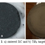
In the sputtering process, the sintered target of SiC and TiB2 acts as a cathode and was kept opposite to the substrates in an evacuated chamber. The base pressure was in the range of 10-6 Torr. Argon is used as a precursor gas due its compatibility with engineering materials, its inertness and low cost. The pressure after Ar introduction is usually between 1 to 10 Pa (1Pa = 0.0075 Torr). The target is at a negative potential and invites argon ion bombardment.2-4 A sintered SiC and TiB2 target is shown in Fig 1.
Figure 1: a) sintered SiC and b) TiB2 target
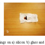
Figure 2: SiCN coatings on a) silicon b) glass and c) 304SS substrates
SiCN coatings were deposited on silicon (100), glass (borosilicate) and steel (SS304) using nitrogen gas during sputtering as shown in Fig 2, details of which are published previously.4 The Ti-B-Si-C coatings were deposited on Si (100) substrates by magnetron sputtering using a Ti-B-Si-C target. The target was made from TiB2– SiC, TiC, Ti and Si- powder. These coatings showed high hardness and adhesion.3
The different morphological features of the sputter deposited film are shown in Fig 3. The different features are a combined effect of pre substrate features, ion solid interaction and surface diffusion. The dark spots are surface artifacts induced by specimen preparation. Many small cracks and fragments caused by collapse are observed on the surface.
The adatoms coming onto the substrate thermodynamically stabilize themselves. The substrate temperature is helpful in this process as it provides kinetic energy to the atoms producing better quality films. However an increase in deposition time may cause increased stress generation in the films.
Figure 3: (a) Different growth morphologies of sputtered Ti-B-Si-C films under optical microscope and (b) TEM micrograph of Si-C-N coatings showing deposition of nanocrystallites of size 50nm – reproduced with permission [4]
Diffusion of atoms of the compositional elements like C, N or Si takes place through grain boundaries and therefore more efficient for microstructures having thick grain boundaries. Temperature provides the required energy of diffusion. For coatings having nano-sized grains, there is no appreciable diffusion instead particle clustering takes place like in the case of SiC-Si3N4 composites increasing the interfacial strength and enhancing hardness. The TEM micrograph showing deposition of nanocrystallites is shown in Fig 3.4
Nanoindentation
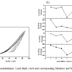
Nanoindentation is a technique to understand the mechanical properties at nanoscale as is particularly helpful for thin films as shallow depth of penetration of the order of nm negates the substrate effect. A three sided pyramidal Berkovich indenter is used for the indentation purpose. The load-depth (P-h) curves during nanoindentation on SiCN /Si are shown in Fig 4 (a). The indentations were performed with a nanosized Berkovich indenter. The Stiffness (S = dP/dh) is determined from the unloading portion of the curve by drawing tangent and finding the slope. The area coming under the load depth cure is a measure of the plastic energy spent during the indentation process. The stiffness obtained is used in determining the elastic modulus whereas the hardness is determined from the projected area. The advantage of this method lies in the fact that indentation area is measured indirectly from depth of penetration and we obtain a continuous hardness and modulus profile with depth. The corresponding average modulus and hardness as well as the values during unloading are shown in Fig 4 (b).A linear unloading region is also observed at the end of the load depth cures. The linear unloading arises due to push back of the buckled region just beneath the indenter.5
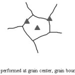
Hardness is determined as the ration of load and the projected area determined indirectly from the depth of penetration. The curves were not coincident which indicating there was a difference in contact area. The reason of such observation is due to the fact that the indentation is not always inside a grain but can also take place at the grain boundaries and triple junctions as shown in Fig 5.6 The grain boundaries are sources of dislocations and dislocation pile ups. As there is no crystallographic orientation of the grain boundaries (GBs), the dislocations find it easier to propagate from the GBs to the grain canter rather than from the grain centre to the grain boundary. Hence indentation performed at grain boundaries or triple junctions give lower values of hardness. The difference in grain and grain boundary hardness is also related to the stress developed during the deposition. A film in a highly stressed state leads to higher variation in hardness and may even lead to fracture after indentation. We obtain a hardness range of 14 – 18 GPa. A new parameter ΔH/H = Hmax – Hmin/Hmax = 0.22 can be introduced which can be called as the hardness deviation factor.
Figure 4: Nanoindentation Load-depth curve and corresponding Hardness and Modulus values
Figure 5: Nanoindentation performed at grain center, grain boundary and grain junction
Similar to hardness, the modulus variation tool place from 150-190 GPa. Therefore, a similar variation takes place in elastic modulus can be parameterized as ΔE/E = Emax – Emin/Emax = 0.21 called the modulus variation factor. The mechanical anisotropy usually gets reflected in modulus variation.
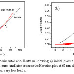
On a closer look at nanoindentation, the initial part of the loading in the elastic regime is according to Hertzian Law P = 4/3Eh3/2√Rwhere P is the load, h the penetration depth, E is the elastic modulus and R is the radius of the indenter. We compared the experimental load-depth response with a simulated Hertizian load depth response as shown in Fig 6(a). The deviation from Hertzian behavior indicates plastic deformation,7 which starts at very low loads (almost from the starting point) as shown separately in Fig 6(b). Interestingly at around 65 nm (shown by arrow) the experimental curve gets passed the Hertzian curve which indicates strain hardening.
Figure 6 :Load-depth curves – experimental and Hertzian showing a) initial plastic deformation as the experimental curve deviates from the Hertzian cure and later crosses the Hertzian plot at 65 nm due to strain hardening and b) the initiation of plastic deformation at very low loads
Conclusions
Ceramic nanocomposite thin films based on Si, C, N, Ti and B with high hardness were deposited using magnetron sputtering. Different growth morphologies were observed on the coating surface due to different phenomenon occurring during sputtering. Nanoindentation showed high hardness of these coatings. The deviations in H and E values were attributed indentation positions, thin film stress and anisotropy. Evidence of strain hardening was found during loading
Acknowledgement
The experimental part has been carried out at CSIR-National Metallurgical Laboratory. The author acknowledges Dr. Suman K. Mishra for the experiments.
Reference
- Palmero P. Nanomaterials. 2015;5:656-696.
CrossRef
- Bhattacharyya A. S.,Mishra S. K. J. of Micromech. & Microengg. 2011;21:015011 and references within.
- Mishra S. K., Bhattacharyya A. S., Mahato P., Pathak L. C. Surf. & Coat. Technol. 2012;207:19-23.
CrossRef
- Bhattacharyya A. S., Mishra S. K., Das G. C., Mukherjee S. Eur. Coat. J. 2009;3:108-114.
- Bull S. J. Nanoindentation of Coatings. J. Phys. D: Appl. Phys. 2005;38:393–413.
CrossRef
- Sha Z. D.,Wan Q., Pei Q. X., Quek S. S., Liu Z. S., Zhang Y. W & Shenoy V. B. Scientific Reports. 2014;4:7437.
CrossRef
- Sun J., Ma A., Jiang J., Han J., Han Y. J. Appl. Phys. 2016;119:095904.
CrossRef

This work is licensed under a Creative Commons Attribution 4.0 International License.

![Fig 3: (a) Different growth morphologies of sputtered Ti-B-Si-C films under optical microscope and (b) TEM micrograph of Si-C-N coatings showing deposition of nanocrystallites of size 50nm – reproduced with permission [4]](http://www.materialsciencejournal.org/wp-content/uploads/2017/06/Vol14_No1_Cocr_Man_Fig3-150x150.jpg)