Effect of Nb Doping on Morphology, Optical and Magnetic Behaviors of Ultrasonically Grown Zno Nanostructures
U. Pal,1*  N. Morales-Flores,2 and E. Rubio-Rosas3
1Instituto de Física, Universidad Autónoma de Puebla, Apdo. Postal J-48, Puebla, Pue. 72570, Mexico.
2Centro de Investigación en Dispositivos Semiconductores, ICUAP, Universidad Autónoma de Puebla, Puebla, Pue. 72570, Mexico.
3Centro Universitario de Vinculación y Transferencia de Tecnología, Benemérita Universidad Autónoma de Puebla, 24 sur y Av. San Claudio, Col. San Manuel, Puebla, Pue. 72570, Mexico
Corresponding author Email: upal@ifuap.buap.mx
DOI : http://dx.doi.org/10.13005/msri/140201
Article Publishing History
Article Received on : 13 Sep 2017
Article Accepted on : 20 Sep 2017
Article Published : 28 Sep 2017
Plagiarism Check: Yes
Article Metrics
ABSTRACT:
ZnO nanostructures containing doped with different atom % of Nb are fabricated through ultrasound assisted hydrolysis in water. Effects of Nd incorporation on the structure, morphology, defect structure, optical, and magnetic behaviors of the nanostructures have been studied utilizing X-ray diffraction, scanning electron microscopy, photoluminescence spectroscopy and magnetometry. We demonstrate that while Nb incorporation in ZnO nanostructures drastically modify their morphology and crystallinity, it does not affect the band gap energy of of ZnO significantly. While Nb incorporation in small concentration creates higher oxygen vacancy related defects in ZnO nanostructures, which are responsible for their visible emissions, incorporation of Nb in higher concentration reduces those defect structures from the band gap of the nanostructures. While oxygen vacancies have been frequently associated to the ferromagnetic behavior of ZnO nanostructures, our results indicate that a mere presence of oxygen vacancy in Nb-doped ZnO nanostructure does not guaranty their ferromagnetic behavior.
KEYWORDS:
Magnetic properties; Nb doping; Optical; Optoelectronic; ZnO nanostructure; Structure.
Copy the following to cite this article:
Pal U, Morales-Flores N, Rubio-Rosas E. Effect of Nb Doping on Morphology, Optical and Magnetic Behaviors of Ultrasonically Grown Zno Nanostructures. Mat.Sci.Res.India;14(2)
|
Copy the following to cite this URL:
Pal U, Morales-Flores N, Rubio-Rosas E. Effect of Nb Doping on Morphology, Optical and Magnetic Behaviors of Ultrasonically Grown Zno Nanostructures. Mat.Sci.Res.India;14(2). Available from: http://www.materialsciencejournal.org/?p=6010
|
Introduction
Zinc oxide (ZnO) is a direct band gap (3.37 eV at room temperature), non-toxic, n-type semiconductor of hexagonal wurtzite structure,1 considered as one of the most promising materials for optoelectronic applications. Wide band gap and large exciton binding energy (60 meV) make it an excellent candidate for several applications such as gas sensor, photodiode, and catalyst,2-4 especially in nanostructure forms. While ZnO nanostructures of different morphologies have been fabricated using a variety of physical and chemical techniques such as radio frequency (RF) sputtering, spray pyrolysis, pulsed laser deposition (PLD), hydrothermal, sol-gel, sonochemical, etc.5-7 both the morphology and intentionally incorporated impurities are seen to affect their structural, optical, and optoelectronic properties8,10 drastically. Substituting Zn ions from their lattice sites by the ions of group III elements such as Al, Ga, and In, n-type ZnO nanostructures of excellent optical quality and low resistivity have been fabricated,11,13 On the other hand, incorporation of group I elements of smaller ionic radii such as Li, Na and K, which occupy the interstitial sites of ZnO lattice has seen to improve the luminescent emissions in ZnO nanostructures.14
Recently, Nb has attracted much attention as a dopant for transparent conducting oxides (TCOs) due to superior electrical and optical properties of Nd-doped TCO thin films.15,16 It is well demonstrated that by incorporation of Nb in ZnO nanoparticles17 it is possible to achieve similar carrier (electron) concentrations as of other common group III dopants with a lower cation substitution, which results in a lower structural disorder and lower lattice deformation. On the other hand, Nb doping in ZnO is quite attractive as there is a valency difference of three between Nb5+ and Zn2+ ions, thereby each incorporated Nb atom can contribute more than one electron to the electrical conductivity of ZnO host.17 Therefore, it is worthwhile fabricating ZnO nanostructures with different Nb contents to study the effect of Nb on their optical, structural, and magnetic properties, to explore their practical applications.
In this article, we report on the fabrication of well-crystalline undoped and Nb-doped ZnO nanostructures by sonochemical technique and their structural, morphological, optical, and magnetic properties. ZnO nanoparticles containing nominal 0.0, 1.0, 2.0, and 5.0 mol % Nb were prepared by ultrasound assisted hydrolysis of zinc acetate, keeping all other parameters like pH of the reaction mixture, concentration of zinc precursor, sonication time, and temperature of reaction fixed. The effects of Nb incorporation on the structural, morphological, magnetic and optical properties of the fabricated ZnO nanostructures have been investigated.
Experimental
Undoped and Nb-doped ZnO nanostructures were synthesized by sonochemical technique, using deionized (DI) water as solvent. Zinc acetate dihydrate [Zn(CH3COO)2•2H2O, Baker, 99.9%], niobium (V) chloride [Sigma Aldrich, 99.4 %], ethylenediaminetetraacetic acid [EDTA, Sigma Aldrich, 99.4%], and ammonium hydroxide [NH4OH, EMD, 29%], were used for preparing the precursor solutions. For preparing the nanostructures, first the aqueous solutions of niobium chloride were prepared by dissolving particular amounts (0.0, 1.0, 2.0, or 5.0 mol % niobium precursor) in 200 ml of DI water at room temperature. Keeping the previous solution under vigorous magnetic stirring, 3.0 g of zinc acetate dihydrate was added. After about 20 min of agitation, 0.5 g of EDTA was added to the reaction mixture. Keeping the mixture solution under magnetic agitation for another 15 min, its pH was measured. The pH of the solution was then adjusted to 7.5 (using a pH meter pH120, conductronic) by drop-wise addition of appropriate amount of NH4OH. After keeping the mixture solution under stirring for about 15 min, it was subjected to ultrasonic irradiation through a T-horn ultrasonic processor (UP400S, Hielscher, 400 Watt, 24 kHz) at 40 W dissipated power under argon gas flow for 3 h. Finally, the obtained product was centrifuged (8000 rpm, 10 min), washed several times with ethanol, and dried at 70 °C for 6 hours in a muffle furnace, obtaining powder samples. Several samples were prepared under similar conditions varying only the amount of the niobium chloride (0.0 – 5.0 mol % nominal) in the reaction mixture.
All the samples were analyzed by X-ray diffraction (XRD) (Bruker AXS D8 Discover diffractometer, with monochromatic CuKa radiation (l=1.5406Å), field emission high resolution scanning electron microscopy (FE-HRSEM) (Zeiss, Auriga 3916), diffuse reflectance spectroscopy (DRS) in UV-Vis spectral range, magnetometry (PPMS, Dynacool-9, Quantum Design) and photoluminescence (PL) spectroscopy.
Results and Discussion
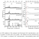
Figure 1 shows XRD patterns of undoped and Nb-doped ZnO nanostructures with different nominal Nb contents (0.0, 1.0, 2.0 and 5.0 mol %). All the samples revealed several clear and intense diffraction peaks, matching well with the wurtzite phase of ZnO (JCPDS Card No. 089-1397). No peak correspond to other phase of ZnO or niobium oxide was revealed in the XRD patterns, suggesting the formation of ZnO in pure wurtzite phase. While the high crystallinity of the undoped ZnO nanostructures is manifested by the presence intense and narrow diffraction peaks, the diffraction peaks became broader and their intensity decreased gradually with the increase of Nb content (Table 1). Moreover, the position of the diffraction peaks shifted towards higher angles on incorporating Nb in ZnO. The average grain size (t) in the ZnO nanostructures was estimated using the Debye Scherrer equation18 considering both the (002) & (101) diffraction peaks:
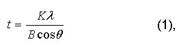
where K is the shape factor, considered to be 0.9, l is the wavelength of used X-ray (λ=1.5406Å), B is the full width at half maximum (FWHM) of the diffraction peak, and θ is the Bragg angle. Estimated average grain size values for the ZnO nanostructures containing 0.0, 1.0, 2.0 and 5.0 mol % of Nb were about 41, 38, 32 and 40 nm, respectively (Table 1). The decrease of peak intensity a considerable change in average grain size in the nanostructures indicates the formation of structural defects on Nb incorporation.
Figure 1: a) XRD patterns of the undoped and Nb-doped ZnO nanostructures, and (b) a close view of the position of (002) and (101) peaks. The dashed red line presents the positions of (002) and (101) peaks in undoped ZnO nanostructures, demonstrating peak shift due to Nd doping.
From the EDS results presented in Table 2, we can see that only 0.0, 1.58, 2.1 and 4.58 at % of Nb were incorporated in the ZnO nanostructures for the nominal 0.0, 1.0, 2.0 and 5.0 mol % of Nb in the reaction mixture. As the ionic radius of Nb+5 (0.64 Å)17 is slightly smaller than the ionic radius of Zn2+ (0.74 Å), incorporation of Nb in ZnO nanostructures does not affect drastically their average grain size. Therefore, the observed higher angle shift of the XRD peaks (Fig. 1) and subsequent change in their lattice constant (“a” & “c”) values (Table 1) cannot be associated to any substantial distortion of ZnO lattice by Nb doping; rather, it can be assigned to the charge imbalance occurred at the substituted cation (Zn2+) sites by the Nb5+ ions. In fact, Zhang et al. in their study on ZnO nanoparticles doped with Al3+ observed a shift of 0.40º towards a higher angle than that of the undoped ZnO nanoparticles, which they attribute to the lattice shrinkage caused by the Al3+ replacing the Zn2+ ions.19 Jan et al. also observed a peak shift towards higher angles in ZnO nanostructures doped with Sn+4, which they attributed to the incorporation of Sn+4 into ZnO lattice and the reduction of strain.20 Moreover, Mote et al. studied ZnO nanocrystals doped with Cr and saw that the XRD peaks of ZnO shift towards higher angles with increasing Cr concentration, attributing such shifts to the lattice expansion due to the Cr substitution for Zn in ZnO crystal lattice.21 It should also be noted that although a high oxygen content in all the samples was detected in their EDS analysis (Table 2), although no diffraction peak associated either to ZnO2 or Nb2O5 could be detected in the XRD spectra of the nanostructures. The fact indicates the higher oxygen content in the samples is due to physisorption at nanostructure surface.
Table 1: Position and FWHM of the main diffraction peaks, estimated average grain size and lattice parameters for the fabricated undoped and Nb-doped ZnO nanostructures.
| |
Difraction peak (101)
|
Difraction peak (002)
|
Lattice contants
|
|
Sample
|
2 θ (deg.)
|
FWHM (deg.)
|
t (nm)
|
2 θ (deg.)
|
FWHM (deg.)
|
t (nm)
|
a
(Å)
|
c
(Å)
|
|
0% Nb
|
36.06
|
0.203
|
41
|
34.26
|
0.209
|
40
|
3.270
|
5.235
|
|
1% Nb
|
36.18
|
0.217
|
38
|
34.37
|
0.216
|
38
|
3.259
|
5.218
|
|
2% Nb
|
36.18
|
0.265
|
32
|
34.36
|
0.267
|
31
|
3.259
|
5.220
|
|
5% Nb
|
36.2
|
0.207
|
40
|
34.37
|
0.218
|
38
|
3.257
|
5.218
|
| |
|
|
|
|
|
|
|
|
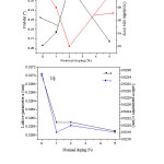
Figure 2a shows the variation of FWHM and average grain size of ZnO nanostructures containing different concentrations of Nb. The average grain size calculated by Scherrer equation is observed to decrease from 41 nm to 32 nm as the Nb content increased from 0 to 2 mol % and then increased to 40 nm for the sample with 5 mol % of Nb. As can be seen, with the increase of Nb %, the FWHM of the main diffraction peaks increase and then decrease, reaching to maximum value of about 0.265 for 2% Nb. On the other hand, incorporation Nb in ZnO lattice is seen to affect its lattice constants. As can be seen from Fig. 2b, in general, incorporation of Nb5+ ions (of smaller ionic radius in comparison to Zn2+ ions) reduces both the lattice constants “a” and “c” of hexagonal ZnO lattice. While the incorporation of a smaller amount of Nb5+ ions causes a sharp reduction of both the lattice constants, incorporation of Nb5+ ions in higher concentrations does not alter much the values of lattice constants further, probably due to a limited substitution capacity of Nb5+ ions due to charge imbalance at cationic lattice sites.
Figure 2: Variation of a) lattice parameters “a” and “c”, b) FWHM and grain size of undoped and Nb-doped ZnO nanostructures.
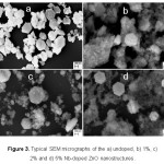
Fig. 3 presents typical SEM images of the Nb-doped ZnO nanostructures containing different nominal concentrations of Nb. As can be seen, the morphology of the nanostructures changes drastically with the increase of Nb content in the samples. While the formation of hexagonal nano-disks with an average diameter of about 490 nm and thickness of about 90 nm can be clearly observed (Fig. 3a) for the undoped sample, spherical nanoparticles of smaller dimensions (40-100 nm) along with a few bigger hexagonal disks were formed in the Nb-doped samples (Figs. 3b-3d). The results indicate that incorporation of Nb5+ ions in ZnO lattice inhibits its normal epitaxial growth along polar surfaces, probably due to the disturbance of normal surface charge balance among the polar planes of ZnO.
Figure 3: Typical SEM micrographs of the a) undoped, b) 1%, c) 2% and d) 5% Nb-doped ZnO nanostructures.
Table 2: EDS estimated elemental composition of the undoped and Nb-doped ZnO nanostructures.
|
Sample
|
O (at. %)
|
Zn (at. %)
|
Nb (at. %)
|
Eg (eV)
|
|
0 % Nb
|
61.2
|
38.8
|
0
|
3.25
|
|
1 % Nb
|
61.54
|
36.88
|
1.58
|
3.27
|
|
2 % Nb
|
67.66
|
30.24
|
2.10
|
3.29
|
|
5 % Nb
|
66.35
|
29.05
|
4.60
|
3.28
|
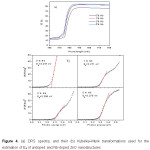
The UV-Vis diffuse reflectance spectra of the ZnO samples prepared with different Nb contents are presented in figure 4. The spectra of all the samples revealed sharp absorption edge in between 375 to 425 nm, characteristic of crystalline ZnO. While, in general, the reflectance of the ZnO nanostructures beyond 425 nm increased with Nb doping, the absorption edge of the nanostructures shift gradually towards lower wavelengths until 2 mol % (nominal) of Nb and then return to higher wavelengths for 5 mol % Nb. The band gap energy (Eg) of the ZnO nanostructures was estimated through Kubelka-Munk (K-M) treatment22 on their DRS spectra (Fig. 4b) from the intersection between the linear fit of the K-M function and the energy axis of the [F(R)hn]2 vs. hn plots (h is the plank constant and n is the frequency of photon). The estimated band gap energy (direct transition) values for the ZnO nanostructures prepared with 0.0, 1.0, 2.0 and 5.0 nominal % of Nb were 3.25, 3.27, 3.29 and 3.28 eV, respectively (Table 2). While the band gap energy of all the Nb-doped ZnO nanostructures are higher than the undoped ones, a small decrease observed for 5 mol % Nb-doped sample, probably due to the presence of Nb5+ ions in excess, causing the formation of Nb clusters, affecting the band gap energy, as substitutional metal ion dopants can introduce electronic states at the bottom of the conduction band, effectively narrowing the band gap of a semiconductor. Such a lower energy shift of band gap in ZnO nanostructures has been observed by several authors due to metal ion doping.17,23,24 Although the particle size of a semiconductor nanocrystal can affect its band gap energy25 due to quantum confinement effect, none of the fabricated samples contain nanostructures smaller than the exciton Bohr diameter of ZnO (⁓5.74 nm) to consider the size effect in the fabricated nanostructures.
Figure 4: (a) DRS spectra, and their (b) Kubelka–Munk transformations used for the estimation of Eg of undoped and Nb-doped ZnO nanostructures.
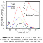
To evaluate the optoelectronic properties of the undoped and Nb-doped ZnO nanostructures, their room temperature PL spectra were recorded. The PL spectra (Fig. 5) of the samples were normalized to their excitonic (UV) emissions for monitoring the intensity variation of visible emission, which is the signature of defect structures in ZnO. PL spectra of all the samples revealed two emission bands. While the ultraviolet (UV) emission around 380 nm generally assigned as the near band edge emission attributed to free excitonic transitions, the broad intense emission in the visible region (centered around 580 nm) has been associated to the structural defects and impurities of different natures. Commonly this broad visible emission contains several component emissions such as blue (2.60 eV), green (2.40 eV), yellow (2.20 eV), orange (1.95 eV), and red (1.75 eV); each associated to particular defect or defect complex in the electronic band gap of ZnO. Several authors have investigated the luminescence properties of ZnO, frequently associating the green component to oxygen vacancies (VO) and zinc vacancies (VZn).26,27 The origin of the red emission has been associated to the deep level defects associated to oxygen vacancies (VO) and oxygen interstitials (Oi), usually observed in the oxygen rich systems.28 For the origin of the blue emission, a number of hypotheses have been proposed, such as electron transition from VO to the valence band29 or zinc interstitials (Zni) to VZn.30 On the other hand, the origin of orange emission has been ascribed to Oi,31,32 and the origin of yellow emission has been ascribed to extrinsic impurity or defects.33,34
Figure 5: Room temperature PL spectra of undoped and Nb-doped ZnO nanostructures. The inset shows the variation of IVis/IUV intensity ratio with Nb content in the samples.
From the normalized PL spectra presented in figure 5, we can see that the relative intensity of the visible emission changes with Nb content in the samples. The IVis/IUV ratio (inset of Fig. 5) increases drastically for the sample containing 1% Nb, compared to the other samples. The ratio decreases with the further increase of Nb content in the samples and become smaller than the undoped sample for the sample containing 5% Nb. Such a variation of IVis/IUV ratio in the nanostructures indicates that, the native defects, especially oxygen vacancies in the nanostructures increase drastically due to the incorporation of Nb ions in ZnO lattice in smaller concentration. However, a higher amount of Nb incorporation apparently reduces VO concentration in the ZnO lattice. The concentration of VO related defects in ZnO lattice can be reduced even lower to the concentration in pristine or undoped ZnO for a nominal Nb concentration of 5 mol %. While the variation of IVis/IUV ratio with Nb concentration in the samples clearly indicates that Nb incorporation in ZnO lattice drastically affects its defect structures, the mechanisms involved appears to be complex, especially in nanostructures. In fact, Kim et al. have studied the photoluminescence of Nb-implanted ZnO films, and observed a similar reduction of native defect concentration, which they attributed to Nb implantation and subsequent thermal annealing.35 As can be noticed from Table 2, the EDS analysis of the samples indicates the presence of excess oxygen in all the nanostructures. In fact, the atom % of oxygen increases with the increase of Nb content in the samples. On the other hand, the atom % of Zn also decreases, discarding the possibility of Zni formation due to Nb doping. Therefore, while an increase in oxygen content in the samples (EDS results) clearly indicates physisorption of oxygen at the surface of the nanostructures, which is proportional to their specific surface area, the reduction of visible emission intensity with increasing Nb content indicates a reduction of defect structures, which is dominated by oxygen vacancies in the ZnO nanostructures.
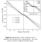
To evaluate the effect of Nb doping on the magnetic response of the ZnO nanostructures, the mass magnetization of undoped and Nb-doped ZnO nanostructures were measured by applying magnetic fields in between -18.0 and +18.0 kOe at room temperature (Fig. 6). The magnetization versus applied magnetic field (M-H) curves of all the nanostructures revealed linear variation of magnetization opposite to the applied magnetic field with small gradients, and very small susceptibility (~ -10e-5), typical for diamagnetic materials36 and of bulk ZnO.3 Frequently, a ferromagnetic behavior has been observed in thin films and nanostructures of metal oxides such as TiO2, HfO2, In2O3, CeO2 and ZnO, which has been associated to oxygen vacancies in them.38-42 As a proof, Hong et al.40 have demonstrated a drastic reduction of magnetic moment of their ferromagnetic Cr-doped ZnO film by annealing them in oxygen atmosphere. In fact, oxygen annealing of the films caused a total loss of ferromagnetic ordering turning them to diamagnetic. On the other hand, by thermal annealing in reducing atmosphere for few hours, the diamagnetic moment of TiO2 and HfO2 films could be increased.43 The room temperature ferromagnetic behavior of these low-dimensional metal oxide structures has been assumed to be due to the exchange interaction between localized spin moments of the surface residing oxygen vacancies.44
As can be seen in Figure 5, apparently all the nanostructures fabricated in the present study exhibit diamagnetic behavior. EDS elemental analysis (Table 2) of all the samples revealed a high oxygen content in the nanostructures, much more than their expected stoichiometric values, along with a reduction of Zn % with the increase of Nb content. While the reduction of atom % of Zn in the nanostructures with increasing Nb % is expected due to substitutional replacement of Zn from lattice sites, the increase of oxygen atom % in the Nb-doped nanostructures is probably due to enhanced adsorption of oxygen at the surface of the nanostructures. The reduction of the size of the nanostructures with increasing Nb content enhances the specific surface area of the samples, thereby increasing the concentration of adsorbed oxygen at their surface.
The inset of Figure 6 shows a zoom-in image of M-H curve at low-field region. As can been seen from the inset, the magnetization curve of the undoped ZnO sample has a small hysteresis and hence a coercivity in the low magnetic field region, similar to a ferromagnetic material. Formation of such hysteresis, even with a small coercive filed in the nanostructures clearly indicates the presence of oxygen vacancies in them, although in smaller concentration. On incorporation of Nb in the nanostructures in smaller concentrations (e.g. 1 mol % nominal) opens up the hysteresis a bit, indicating an enhancement of oxygen vacancy concentration in the nanostructures, as has been observed in their PL spectrum. However, incorporation of Nb in higher concentration reduces the concentration of oxygen vacancies making the nanostructures more diamagnetic. In fact, the magnetic behavior of the Nb incorporated nanostructures are in good agreement with their PL spectra presented in Fig. 5.
Figure 6: Magnetization versus magnetic field of undoped and Nb-doped ZnO nanostructures. The inset shows a zoom-in image at low-field region.
While the transition metal-doped metal oxides, which behave as dilute magnetic semiconductor (DMS) have been studied extensively due to their potential applications in spintronics, their magnetic behaviors remained unclear due to the contradictory results published in the literature.45,46 It seems the method of fabrication plays a substantial role on the magnetic behavior of DMS, especially in their nanostructure forms.41,45, 47-49 As has been discussed earlier, due to smaller ionic radius, Nb5+ ions can easily substitute Zn2+ ions from the lattice sites of ZnO up to a certain concentration, without significant distortion of charge balance and metal ion coordination. These substitutionally incorporated Nb5+ ions would increase the oxygen vacancy concentration in ZnO lattice due to their higher oxidation state than the original Zn2+ ions. A further incorporation of Nb5+ ions in ZnO lattice probably causes the formation ion complex between the singly ionized oxygen vacancies and Nb5+ ions with a strong local interaction between the Nb spins and the vacancies, as demonstrated by Chambers et al. for Co-doped titania films50 through near-edge and extended x-ray absorption fine structure analysis. While the formation of such ion complex will shift the oxygen vacancies towards substituting Nb5+ ions of the lattice due to strong electrostatic interaction, the availability of free electron from the ionized oxygen vacancy, which is supposed to be the principal reason form DMS behavior of transition metal doped metal oxide47 would be limited. However, as the fabricated Nb-doped nanostructures do not bear a well-defined shape and dimension, it is difficult to monitor the effects of surface adsorbed oxygen and formed ion complexes, which needs a further extensive study.
Conclusions
In summary, we present a facile sonochemical technique for the fabrication of ZnO nanostructures containing different Nb contents. It has been demonstrated that the incorporation of Nb in ZnO nansotructures not only affect their morphology and dimensions, but also affect their emission and magnetic behavior drastically. While the incorporation of Nb does not affect band gap energy of the nanostructures significantly, it helps to reduce electronic defect levels from their band gap, enhancing the relative intensity of excitonic emissions, i.e. enhances their optoelectronic quality. While the incorporation of Nb in smaller concentration (e.g. 1 mol % nominla) enhances the oxygen vacancy induced ferromagnetic behavior of ZnO nanostructures, incorporation of Nb ions in higher concentration eliminates their ferromagnetic behavior due to the formation of Nb ion – oxygen vacancy complexes.
Acknowledgement
The authors acknowledge the financial support extended by VIEP-BUAP, Mexico (grant # VIEP/EXC/2017-257) for the execution of this research work.
References
- Ozgur U., Alivov Y. I., Liu C., Teke A., Reshchikov M. A., Dogan S., Avrutin V., Cho S. J., Morkoc H. A comprehensive review of ZnO materials and devices.J. Appl. Phys. 2005;98:041301.
CrossRef
- Jeong I. S.,Kim J. H., Im S. Ultraviolet-enhanced photodiode employing n-ZnO/p-Si structure. Appl. Phys. Let. 2003;83:2946-2948.
CrossRef
- Zhang Y., Xu J., Xu P., Zhu Y., Chen X and Yu W. Decoration of ZnO nanowires with Pt nanoparticles and their improved gas sensing and photocatalytic performance.Nanotechnology. 2010;21:285501:7.
CrossRef
- Morales-Flores N., Pal U., Mora E. S., Photocatalytic behavior of ZnO and Pt-incorporated ZnO nanoparticles in phenol degradation. Applied Catalysis A: General. 2011;394:269–275.
CrossRef
- Shao J., Dong W., Li D., Tao R., Deng Z., Wang T., Meng G., Zhou S., Fang X. Metal-semiconductor transition in Nb-doped ZnO thin films prepared by pulsed laser deposition. Thin Solid Films. 2010;518:5288–5291.
CrossRef
- Chen C., Yu B., Liu P., Liu J. F., Wang L. Investigation of nano-sized ZnO particles fabricated by various synthesis routes. J. Ceramic Proces. Res. 2011;12:420-425.
- Pal U., Kim C. W., Jadhav N. A and Kang Y. S. Ultrasound-assisted synthesis of mesoporous ZnO nano structures of different porosities. J. Phys. Chem. C. 2009;113:14676–14680.
CrossRef
- Nam S. H., Cho S. J., Boo J. H. Physical properties of metal-doped zinc oxide films for surface acoustic wave application. Nanoscale Res. Lett. 2012;7:25.
CrossRef
- Morales A. E and Pal U. Effect of In Sb and Ga doping on the structure and vibrational modes of hydrothermally grown ZnO nano structures. Current Appl. Phys. 2011;11:525-531.
CrossRef
- Zeferino R. S., Flores M. B., Pal U. Photoluminescence and Raman Scattering in Ag-doped ZnO Nanoparticles. J. Appl. Phys. 2011;109:014308:6.
CrossRef
- Bae S. Y., Na C. W., Kang J. H., Park J. Comparative structure and optical properties of Ga-, In-, and Sn-doped ZnO nanowires synthesized via thermal evaporation.J. Phys. Chem. B. 2005;109:2526-2531.
CrossRef
- Xu L., Su Y., Chen Y., Xiao H., Zhu L., Zhou Q., Li S. Synthesis and characterization of indium-doped ZnO nanowires with periodical single-twin structures.J. Phys. Chem. B. 2006;110:6637-6642.
CrossRef
- Makino T., Segawa Y., Yoshida S., Tsukazaki A., Ohtomo A., Kawasaki M., Koinuma H. Spectral shape analysis of ultraviolet luminescence in n-type ZnO:Ga. J. Appl. Phys. 2005;98:093520:4.
CrossRef
- Potucek Z., Bryknar Z., Ptcaek P., Hubicka Z. Luminescence of defects in Li-doped ZnO thin films. Phys. Stat. Sol. 2005;2:256-259.
CrossRef
- Furubayashi Y., Hitosugi T., Yamamoto K., Inaba K., Kinoda G., Hirose Y., Shimada T., Hasegawa T. A transparent metal: Nb-doped anatase TiO2, Appl. Phys. Lett. 2005;86:252101:3.
CrossRef
- Xu J. W., Wang H., Jiang M. H., Liu X. Y. Properties of Nb-doped ZnO transparent conductive thin films deposited by rf magnetron sputtering using a high quality ceramic target. Bull. Mater. Sci. 2010;33:119–122.
CrossRef
- Lin J. M., Zhang Y. Z., Ye Z. Z., Gu X. Q., Pan X. H., Yang Y. F., Lu J. G., He H. P., Zhao B. H. Nb-doped ZnO transparent conducting films fabricated by pulsed laser deposition. Appl. Surf. Sci. 2009;255:6460-6463.
CrossRef
- Cullity B. D. Elements of X-ray diffraction, Addison-Wesley Publishing Company,.Inc. 1956;98-99.
- Jood P., Mehta R. J., Zhang Y., Peleckis G., Wang X., Siege R. W., Borca-Tasciuc T., Dou S. X., Ramanath G., Al-doped zinc oxide nanocomposites with enhanced thermoelectric properties. Nano Letters. 2011; 11(10):4337–4342.
CrossRef
- Jan T., Iqbal J., Ismail M., Zakaullah M., Naqvi S. H., Badshah N. Sn doping induced enhancement in the activity of ZnO nanostructures against antibiotic resistant S. aureus bacteria.Int. J. Nanomed. 2013 8:3679-3687.
CrossRef
- Mote D., Huse V. R.,Dole N. V. B. Synthesis and characterization of Cr doped ZnO nano crystals.World J. Cond. Mater. Phys. 2011;2:208.
CrossRef
- Morales E. A.,Mora E. S.,Pal U. Use of diffuse reflectance spectroscopy for optical characterization of un-supported nano structures.Rev. Mex. Fís. 2007;S53:18–22.
CrossRef
- Nair M. G., Nirmala M., Rekha K., Anukaliani A. Structural, optical, photo catalytic and antibacterial activity of ZnO and Co doped ZnO nano particles. Mater. Lett. 2011;65:1797–1800.
CrossRef
- Zhang Y., Yang Y., Zhao J., Tan R., Wang W., Cui P., Song W. Optical and electrical properties of aluminum-doped zinc oxide nano particles.J. Mater. Sci. 2011;46:774–780.
CrossRef
- Wang N., Yang Y and Yang G. Great blue-shift of luminescence of ZnO nanoparticle array constructed from ZnO quantum dots. Nanoscale Res. Letts. 2011;6:338:6.
- Zhao Q. X., Klason P., Willander M., Zhong H. M., Lu W., Yang J. H. Deep-level emissions influenced by O and Zn implantations in ZnO. Appl. Phys. Lett. 2005;87:211912:3.
- Yamauchi S., Goto Y., Hariu T. Photoluminescence studies of undoped and nitrogen-doped ZnO layers grown by plasma-assisted epitaxy. J. Cryst. Growth. 2004;260:1–6.
CrossRef
- Wu L., Wu Y., Pan X., Kong F. Synthesis of ZnO nanorod and the annealing effect on its photoluminescence property.Opt. Mater. 2006;28:418–22.
CrossRef
- Zhang L., Yin L., Wang C., Lun N., Qi Y., Xiang D. Origin of visible photoluminescence of ZnO quantum dots: Defect-dependent and size-dependent.J. Phys. Chem. C. 2010;114:9651-9658.
CrossRef
- Ahn C. H., Kim Y. Y., Kim D. C., Mohanta S. K., Cho H. K. A comparative analysis of deep level emission in ZnO layers deposited by various methods.J. Appl. Phys. 2009;105:013502:5.
CrossRef
- Studenikin S. A., Golego N., Cocivera M. Fabrication of green and orange photoluminescent, undoped ZnO films using spray pyrolysis. J. Appl. Phys. 1998;84:2287-2294.
CrossRef
- Wu X. L., Siu G. G., Fu C. L., Ong H. C. Photoluminescence and cathodoluminescence studies of stoichiometric and oxygen-deficient ZnO films. Appl. Phys. Lett. 2001;78:2285.
CrossRef
- Li D., Leung Y. H., Djuriši´c A. B., Liu Z. T., Xie M. H., Shi S. L., Xu S. J., Chan W. K. Different origins of visible luminescence in ZnO nanostructures fabricated by the chemical and evaporation methods. Appl. Phys. Lett. 2004;85:1601-1603.
CrossRef
- Harada Y., Hashimoto S. Enhancement of band-edge photoluminescence of bulk ZnO single crystals coated with alkali halide. Phys. Rev. B. 2003;68045421:4.
CrossRef
- Kim C. O., Shin D. H., Choi S. H. Strongly-enhanced near-band-edge photoluminescence of Nb-implanted ZnO films.J. Cryst. Growth. 2011;326:42-44.
CrossRef
- Robert C. (ed.) West 67th ed. Boca Raton, FL: CRC Press, USA. Inc. 1986;87-64.
- García M. A., Merino J. M., Pinel E. F., Quesada A., De la Venta J., González M. L. R., Castro G. R., Crespo P., Llopis J., González-Calbet J. M., Hernando A. Magnetic Properties of ZnO Nano particles. Nano Lett. 2007;7:1489-1494.
CrossRef
- Hsu H. S., Huang J. C. A., Huang Y. H., Liao Y. F., Lin M. Z., Lee C. H., Lee J. F., Chen S. F., Lai L. Y., Liu C. P. Evidence of oxygen vacancy enhanced room-temperature ferromagnetism in Co-doped ZnO. Appl. Phys. Lett. 2006;88:242507:3.
- Xu X., Xu C., Dai J., Hu J., Li F., Zhang S. Size dependence of defect-induced room temperature ferromagnetism in undoped ZnO nano particles.J. Phys. Chem. C. 2012;116:8813−8818.
CrossRef
- Hong N. H., Sakai J., Huong N. T., Poirot N., Ruyter A. Role of defects in tuning ferromagnetism in diluted magnetic oxide thin films.Phys. Rev. B. 2005;72:045336:5.
- Han X., Lee J., Yoo H. I. Oxygen-vacancy-induced ferromagnetism in CeO2 from first principles.Phys. Rev. B. 2009;79:100403.
CrossRef
- Sundaresan A., Bhargavi R., Rangarajan N., Siddesh U., Rao C. N. R. Ferromagnetism as a universal feature of nanoparticles of the otherwise nonmagnetic oxides. Phys. Rev. B. 2006;74:161306:6.
- Hong N. H., Sakai J., Poirot N., Brizé V. Room-temperature ferromagnetism observed in undoped semiconducting and insulating oxide thin films.Phys. Rev. B. 2006;73:132404:4.
- Barick K. C., Aslam M., Vinayak P. D., Bahadur D. Self-Aggregation and Assembly of Size-Tunable Transition Metal Doped ZnO Nanocrystals. J. Phys. Chem. C. 2008;112:15163.
CrossRef
- Ueda K., Tabata H., Kawai T. Magnetic and electric properties of transition-metal-doped ZnO films, Appl. Phys. Lett. 2001;79:988-990.
CrossRef
- Jedrecy N., von Bardeleben H. J., Zheng Y., Cantin J. L. Electron paramagnetic resonance study of Zn1-xCoxO: A predicted high-temperature ferromagnetic semiconductor.Phys. Rev. B. 2004;69:041308:4.
- Jaffe J. E., Droubay T. C., Chambers S. A. Oxygen vacancies and ferromagnetism in CoxTi1−xO2−x−y, J. Appl. Phys. 2005;97:073908:6.
- Huang B., Zhu D., Ma X. Great influence of the oxygen vacancies on the ferromagnetism in the Co-doped ZnO films. Appl. Surf. Sci. 2007;253:6892-6895.
CrossRef
- Manivannan A., Glaspell G., Dutta P., Seehra M. S. Nature of the reversible paramagnetism to ferromagnetism state in cobalt-doped titanium dioxide.J. Appl. Phys. 2005;97:325.
- Chambers S. A., Heald S. M., Droubay T. Local Co structure in epitaxial CoxTi1-xO2-x anatase,.Phys. Rev. B. 2003;67:100401:4.
CrossRef

This work is licensed under a Creative Commons Attribution 4.0 International License.