Kishor Hurde1*  and A. B. Lad2
1Dept of Physics, Mungasaji Maharaj Mahavidyalaya, Darwha, Dist. Yavatmal
2Dept of Physics, Amolakchand Mahavidyalaya, Yavatmal
Corresponding author Email: drajay_lad@rediffmail.com
DOI : http://dx.doi.org/10.13005/msri/140213
Article Publishing History
Article Received on : 02 Sept 2017
Article Accepted on : 02 Oct 2017
Article Published : 10 Nov 2017
Plagiarism Check: Yes
Article Metrics
ABSTRACT:
The CdO and ZnO are n- type semiconductors are transparent conducting in nature, inexpensive, mechanically stable and highly resistance to oxidation. In the present work these films have been obtained from thermal annealing of chemically deposited CdS and ZnS thin films. The structural properties of chemically deposited CdS and ZnS thin films and thermally annealed CdO and ZnO thin films have been studied. From x-ray diffraction data it is observed that annealing of the thin films at a particular temperature enhance the structural properties.
KEYWORDS:
Annealing; Chemical bath deposition; CdO; Structural properties; ZnO
Copy the following to cite this article:
Hurde K, Lad A. A. Study of Structural Properties of Annealed CdO and ZnO thin films. Mat.Sci.Res.India;14(2)
|
Introduction
CdO and ZnO is an n-type semiconductor belonging to II-VI group of periodic table. These materials possess wide band gap of approximately 2.4eV and 3.3eV at room temperature. These films are semitransparent in nature have been widely used in a flat panel displays, solar cells and gas sensing applications. These films are transparent conducting in nature, inexpensive, mechanically stable and highly resistance to oxidation.1-5 The CdS and ZnS thin films prepared by chemical bath deposition technique have been extensively studied by many researchers. In the present work we have attempted to annealed CdS and ZnS films prepared by chemical bath deposition to form CdO and ZnO thin films.
The CdO and ZnO films obtained by annealing were characterized for investigation of structural properties. It is observed that annealing effect improve structure of thin films.6 -7
Experimental
For the preparation of CdS and ZnS thin films chemical bath deposition technique were utilized. In this apparatus there is a facility for rotating the substrate, stirring the solution using the magnetic stirrer, change the temperature of the entire assembly and stabilized it at a particular value etc. In order to get uniform film thickness the film substrate is continuously rotated and the solution is continuously stirred using magnetic stirrer. The temperature of assembly is maintained by heating arrangement and temperature controller. The thickness of the films governed by controlling the deposition time and the concentration of the solution.8-9-10
The prepared samples of CdS and ZnS by chemical bath deposition were taken for annealing and kept into muffle furnaces Biotech of India of 2500 watts at 15 amperes which can withstand maximum temperature of 10000c. The temperature of the furnaces was maintained at 6000c for more than 8 hours. After annealing sulfide ions converted into oxide ions by converting CdS into CdO and ZnS into ZnO.11-12
The prepared films of CdO and ZnO with annealing effect were taken for characterization to determine structural properties.
Result and Discussion
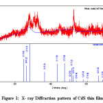
Figure 1: X- ray Diffraction pattern of CdS thin film
Table 1: XRD data of CdS thin film
|
No.
|
2theta (deg)
|
d(ang)
|
Height (CPS)
|
FWHM(deg)
|
Grain size (nm)
|
Lattice strain
|
|
1
|
27.94
|
3.910
|
57
|
1.68
|
5.09
|
0.0295
|
|
2
|
32.25
|
2.774
|
72
|
4.9
|
1.76
|
0.0740
|
|
3
|
52.67
|
1.736
|
99
|
0.59
|
15.7
|
0.0052
|
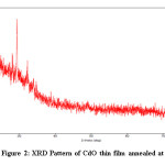
Figure 2: XRD Pattern of CdO thin film annealed at 6000C
Table 2: XRD data of CdO thin film annealed at 6000C
|
Sr.
No.
|
2theta
(deg)
|
d(ang)
|
FWHM
|
Grain size
(nm)
|
Lattice
strain
|
|
1
|
29.32
|
3.043
|
0.164
|
52.32
|
0.0027
|
|
2
|
32.47
|
2.7545
|
0.163
|
53.04
|
0.0024
|
|
3
|
34.017
|
2.633
|
0.163
|
53.26
|
0.0023
|
|
4
|
49.230
|
1.849
|
0.163
|
56.01
|
0.0016
|
Figure 1 show the X- Ray diffraction pattern of CdS thin film obtained using X-Ray generated at 40kv energy and 15mA current without filter. SC 70 detector with the continuous scan mode was used. Qualitative Analysis Result shows that the Phase Name of the film is Greenokite with the formula CdS having DB Card number 1011054. The peak list of the CdS sample is shown in table 1.13,14
The thermally oxidized CdO thin film were obtained by annealing the CdS as-depodited at 6000C for more than 8 hours. The X- Ray diffraction data obtained for CdO thin film given in the table 2 and X- ray reflection peaks shown in figure 2 It is seen from the table 2 that the annealing temperature changes the grain size. The prominent reflection peaks are observed at the annealing temperatur 6000C as seen in figure 2. The 2theta values corresponds to the particular reflection planes indicating the formation of CdO nanoparticle having pure hexagonal structure which matches with the standared JCPDF data.15,16
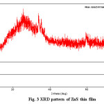
Figure 3: XRD pattern of ZnS thin film
The XRD pattern of the ZnS thin film was investigated by the Regaku Mimflex 600 Model X-ray diffractometer using PDXL software. This pattern explains the structural properties of ZnS film. The XRD pattern of ZnS sample as shown in figure 3 give three prominent peak at 2θ values 32.620, 35.2950, and 37.0770. The d value1.429A0, 1.333A0 and 1.277A0 respectively. These peaks are showing reflection from (100), (002) and (101) planes, indicating the formation of ZnS nano-particles having cubic zinc blend structure. The enhance intensity for the peak corresponding to (002) plane indicating preference orientation along c-axis. The peak list of ZnS sample is shown in Table 3.17
Table 3: XRD data of ZnS thin film
|
No.
|
2theta(deg)
|
d(ang.)
|
Height
(cps)
|
FWHM
(deg)
|
Grain Size (nm)
|
Lattice Strain
|
|
1
|
32.62
|
2.7428
|
416
|
0.22
|
39.31
|
0.0033
|
|
2
|
35.295
|
2.5409
|
642
|
0.199
|
43.76
|
0.0027
|
|
3
|
37.077
|
2.4228
|
729
|
0.262
|
33.44
|
0.0034
|
|
4
|
48.263
|
1.8841
|
159
|
0.27
|
33.69
|
0.0026
|
|
5
|
57.31
|
1.6064
|
128
|
0.37
|
25.56
|
0.0030
|
|
6
|
63.55
|
1.4627
|
190
|
0.30
|
32.54
|
0.0021
|
|
7
|
68.56
|
1.3676
|
80
|
0.47
|
21.36
|
0.0030
|
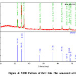
Figure 4: XRD Pattern of ZnO thin film annealed at 6000C
The X- Ray diffraction data obtained for ZnO thin film annealed at 6000C is shown in table 4. The prominent reflection peaks are observed with the reflection from (100) (002) (101) (102) (110) (103) seen in figure 4. This data indicate that annealed ZnO thin film is polycrystalline in nature having pure hexagonal structure as per the DB card number 2300113 and 9040180 respectively. The grain size obtained from the Debye- Scherer’s formula. It is found that average grain size is obtained which changes due to the change in annealing temperature18,19.
Table 4: XRD data of annealed ZnO thin film at 6000 C
|
Sr.
No.
|
2theta
(deg)
|
d(ang)
|
FWHM
|
Grain size
(nm)
|
Lattice
strain
|
|
1
|
31.877
|
2.805
|
0.246
|
35.08
|
0.0038
|
|
2
|
34.513
|
2.596
|
0.223
|
38.98
|
0.0031
|
|
3
|
36.352
|
2.469
|
0.301
|
29.03
|
0.0040
|
|
4
|
47.664
|
1.906
|
0.34
|
26.68
|
0.0034
|
|
5
|
62.901
|
1.476
|
0.404
|
24.08
|
0.0029
|
Conclusion
The thin film of CdO and ZnO successfully obtained by thermal annealing of CdS and ZnS at 6000C. X – ray diffraction analysis of the thermally annealed films CdO film shows that films are polycrystalline in nature The prominent reflection peaks are observed at the annealing temperatur 6000C. The 2theta values corresponds to the particular reflection planes indicating the formation of CdO nanoparticle having pure hexagonal structure. The prominent reflection peaks are observed with the reflection from (100) (002) (101) (102) (110) (103) for ZnO thin film. This data indicate that annealed ZnO thin film is polycrystalline in nature having pure hexagonal structure. It is found that average grain size is obtained which changes due to the change in annealing temperature.
References
- Abou-Ras D. Thomas Kirchartz and Uwe Rau, Advanced Characterization Technique for Thin Film Solar Cells, Wioley- VCH. 2011.
- Pawar S. H.,Bhosale C. H. Bull. Matter Sci. 1986;8(3):419.
CrossRef
- Lokhande C. D. Material Chemistry and Physics. 1991;27:1-43.
CrossRef
- Moualika H.,Hariech S., Aida M. S. Thin Solid Films. 2009;518:1259.
CrossRef
- Ghonein D. J of Optoelect. Adv. Mat. 2010;12:5.
- Nair P. K., Nair M. T. S et al. J. Phys D. 1989;22:829.
CrossRef
- Noikaew B et al. Journal of Metals, Materials and Materials. 2008;18(2):49.
- Borah J. P.,Sarma K. C. Acta Physica Polonica A. 2008;114(4).
CrossRef
- Nadeem M. Y., Ahme W. Turk J Phy. 2008;24:625.
- JCPDS XRD Spectral data files.
- Dr. Eltkayef K. A., Dr. Abbas K. A., Multak M. H. Int. Jou. Of App. Or Inn. In Eng. & Management (IJAIEM). 2015;7.
- Ubale A. U., Wadnerkar S. S.,Sonone P. N & Tayade G. D. Study of Structural, Optical and Electrical Properties of CdO thin film. Archives of Physics Research. 2014;5(6):43-48.
- Mishra R. L., Sharma A. K., Prakash S. G. Gas sensitivity and characterization of Cadmium Oxide (CdO) Semi-Conducting thin films deposited by Spray Pyrolysis technique. Digest J. Nanomater. Bio. Str. 2009;4(3):511–518.
- Abbas K. A., Multak M. H. Int Jou. In Eng. And Management. 2009;5(7)2015.
- Pandya G. S. Influence Of Growth Process On The Properties Of Chemically Prepared Sulphide Thin Films. International Journal of Scientific Research. 2016;(7)12:14765-14768.
- Maske D. Growth and Characterization of CdS Thin Films by Chemical Bath Deposition. International Journal of Scientific and Research Publications. 2016;6(6).

This work is licensed under a Creative Commons Attribution 4.0 International License.