Electrical and Photoluminescence Properties of Mo- doped ZnO Films Deposited by Spray Pyrolysis
T. Sreenivasulu Reddy1, G. Phaneendra Reddy2 , K.T. Ramakrishna Reddy2,*
1Department of Physics, Sir Vishveshwaraiah Institute of Science and Technology, Madanapalle, India.
2Solar Photovoltaic Laboratory, Department of Physics,Sri Venkateswara University, Tirupati-517 502, India.
Corresponding Author E-mail: ktrkreddy@gmail.com
DOI : http://dx.doi.org/10.13005/msri/150303
Article Publishing History
Article Received on : 09-Aug-2018
Article Accepted on : 24-Oct-2018
Article Published : 26 Oct 2018
Plagiarism Check: Yes
Reviewed by: Ashish Kumar
Second Review by: V. S. ANGULAKSHMI
Final Approval by: Faheem Shiekh
Article Metrics
ABSTRACT:
Spray deposited Mo-doped zinc oxide (MZO) films were grown on glass substrates at different substrate temperatures (Ts)that varied in the range of 300°C-450 °C at aconstant Mo-doping concentration of 2 at. %.XRD spectra revealed better crystallinity of films prepared atTs400 °C. FTIR spectra showed the vibrational modes related toZn–O bonding.Photoluminescence spectra of MZO films showed a peakrelated toviolet emissionsbetween 400 nm and 420 nm. Electrical analysis showed n type semiconducting nature of the films and the films grown at Ts= 400 °C hadlow resistivity and high mobility.Adetailed analysis on theeffect of substrate temperatureon photoluminescence and electrical propertiesof MZO films wasdiscussed and reported.
KEYWORDS:
FTIR; Hall Effect; Measurements; Photoluminescence; Spray pyrolysis; Thin films; XRD
Copy the following to cite this article:
Reddy T. S, Reddy G. P, Reddy K. T. R. Electrical and Photoluminescence Properties of Mo- doped ZnO Films Deposited by Spray Pyrolysis. Mat.Sci.Res.India;15(3).
|
Copy the following to cite this URL:
Reddy T. S, Reddy G. P, Reddy K. T. R. Electrical and Photoluminescence Properties of Mo- doped ZnO Films Deposited by Spray Pyrolysis. Mat.Sci.Res.India;15(3). Available from: http://www.materialsciencejournal.org/?p=96251
|
Introduction
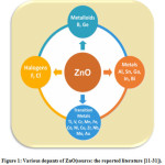
An extensive investigation has been carried out on the transparent conducting oxide (TCO) films for variety of applications in science and technology for many decades.The conventional TCOs for example InO2and SnO2exhibitlow metallic forms while exposed to the hydrogen plasma.1,2 Alternatively, zinc oxide (ZnO) can be used as a prominent TCO material as it can be withstand to the hydrogen plasma.3 Deposition of pure and doped ZnO thin films has attracted much attention because of its low toxicity,wide optical band gap (3.3eV) and high refractive indices.4-10 Till now, the doping of ZnO films using different elements (Fig.1) has been reported.11-31 However, there is less exploration, especially,in the case of MZO films.
The doping of ZnO with Mois very beneficial due to the large valence difference (+4) between Mo6+ and Zn2+ ions. Eachdoped Mo-atom will donate 4 free electrons to the host lattice. Therefore,even alittle bit of Mo-doping can afford more free electrons, which amend the electrical conductivity.32 The preparation of MZO filmshas been reported by various physical and chemical methods.33-38 Among the reported techniques, spray pyrolysis is a significant technique for the deposition of ZnO thin films due to its simplicity,low cost and vacuum free.
The effect of various dopants such as Mg, Co, Ni,Mn, and Ga on the spray deposited ZnO films has been studied thoroughly in our laboratory from fast few years.39-44 To the best of our knowledge, no reports were published on the effect of Ts on the photoluminescence and electrical properties of MZO films deposited using spray pyrolysis technique. An understanding of effect of Ts on the physical properties of MZO films can help to achieve good optoelectrical MZO films to TCO applications. Therefore, in this paper, the effect of Tsonthe photoluminescence and electrical properties of Mo-doped zinc oxide films was analyzed in detail and discussed.
Figure 1: Various dopants of ZnO(source: the reported literature [11-31]).
Experimental
MZOfilms were grown using spray pyrolysis method on glass substrates by changing the Ts in the range, 300 – 450 °Cusing a constant Mo-doping concentration of 2 at. %. Zinc chloride (ZnCl2) (Aldrich 98%) and molybdenumchloride (MoCl5)2 (Aldrich 95%) dissolved in methanol were used as the precursor sources for zinc and Mo respectively. In a typical deposition of MZO films,6 ml/min flow rate of precursor solution was used with 8 l/min of compressed carrier gas, and the distance between the source (from thenozzle)to substrate as 25 cm at an interval of 1 min were maintained. All the deposited Mo-doped ZnO films were pale white in appearance, pinhole free and homogeneous. The scratch tape test revealed that the layers were strongly adherent to the substrates.
The structural properties were studied using a Siefert X-ray diffractometer with a CuKα radiation source (λ=1.542 Å).Fourier transform infrared (FTIR) spectrum of MZO films was recorded in the wavelength range of 500 cm-1-4000 cm-1 using a Thermo Nicolet IR-200 spectrophotometer. The photoluminescence (PL) properties of the films were studied by YVON Florolog-3 (model:FL3-22) with the Xenon flash lamp of 185-2000 nm wavelength as the light source.Hall Effect measurement (model: HMS-3000) setup was used for measuring the electrical properties of the MZO films.
Results and Discussion
Structural Analysis
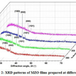
Fig. 2 shows the X-ray diffraction profiles of MZO layers deposited at different substrate temperatures. The XRD patterns revealed that all the as grown films were polycrystalline in nature since they showed more peaks. Films prepared at Ts= 300°C indicated less crystallinity because of incomplete reaction due to insufficient thermal energy. At Ts = 350°C, the films showed better crystallinity with the appearance of two strong peaks, corresponding to (100) and (002) planes of ZnO. However, the films grown at Ts =400°C showed three peaks corresponding to (100), (002),and(101) planes of ZnO with an improved intensity. This indicates the enhancement in the crystallinity of the MZO films.
However, with further increase of temperature to 450°C, there was a change in the preferred orientation and the films exhibited only (002) and (101) peaks with decreased intensity. The observed low crystallinity at such temperatures was attributed to the vaporization of solvent from the droplet before it reaches the substrate surface causing a powdery nature of the films.Further, the crystallite size (D) of MZO films was calculated using Debye-Scherrer formula.The evaluated crystallite size was varied in the range of 112 – 647 nm with the change of substrate temperature. The value of crystallite size was initially increased with temperature and reached to a maximum value of 647 nm at 400°C, there after it was decreased to 396 nm when the temperature was reached to 450°C.
Figure 2: XRD patterns of MZO films prepared at different Ts.
FTIR studies
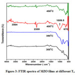
Fig.3 shows the FTIR transmission spectra of MZO films deposited at different substrate temperatures. Normally, the vibrational modes below 1000 cm-1 are used to investigate the infrared active bonding amongst the different inorganic elements present in the films. The peak at 670cm-1 is corresponding to the vibrational energies of Zn–O, which confirms the formation of ZnO phase in all the films. The vibrational mode noticed at 1009.5 cm-1 is evident that the substitution of Mo6+ ions into the ZnO lattice at a substrate temperature of 400°C.The band present at 2308 cm-1 was attributed to the stretching vibration mode of the C=O group, which might be due to the incorporation of atmospheric carbon into the film. Also, the small absorption peak appeared around 3564 cm-1 corresponds to the –OH group of H2O, which indicates the existence of absorbed water on the surface of the MZO films.
Figure 3: FTIR spectra of MZO films at different Ts.
Photoluminescence Studies
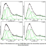
Fig.4 shows the PL spectra of MZO films grown at different substrate temperatures. The deconvolution of PL spectra indicated the peaks that were centered at around 370 nm to 390 nm, 400 nm to 420 nm, and 522 nm to 525nm respectively. The UV luminescence peak (370 nm to 390nm) is corresponding to near-band-edge emission of ZnO. The peak centered between 400nm and 420nm is originated from the coordinative and unsaturated Zn sites in the ZnO. This confirms the existence of Mo impurity atoms in the MZO layer.45-47 Jin et al.,48 noticed a peak at 420 nmfor ZnO films prepared using PLD technique, the observed peak was generated due to the grain boundaries defects of ZnO.Yi et al.,49 also observed the deconvoluted peak at 420 nm for ZnO films because of the electron–hole recombination at defect centers. Therefore, the peak centered between 400nm and 420nm is speculated the existence of Mo impurity atoms in the MZO layers. Abroad peak observed at 522 nm was due to the visible luminescence from oxygen ion defect states in the MZO films. With increasing of substrate temperature, the peak position was slightly shifted towards the right.The intensity and position of these deconvoluted peaks varied with temperature, which could be explained due to the change in intrinsic defect concentration in MZO films. These results are comparable with the data obtained on MZO films grown by chemical spray processusing ZnC4H6O4 as a source for zinc.50-52 Due to the intrinsic change in defect concentration causes variation of physical properties of ZnO films, which is useful in optoelectronic and enhancing the sodium meta phosphate glasses properties.10
Figure 4: Photoluminescence spectra of MZO films (where the coloured lines represent the deconvoluted peaks.)
Electrical properties
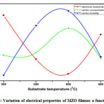
Fig. 5 shows the variation of electrical resistivity (ρ), carrier mobility (μ) and carrier concentration (N) as a function of Ts.The Hall measurements clearly showed that the as-grown MZO films were n-type conducting with the electrical resistivity (ρ), carrier mobility (μ) and charge carrier concentration (N) varying in the range, 9.5×10⁻²– 1.9×10⁻²Ω-cm, 15- 42 cm2/Vs and 4.3×10¹⁸– 7.8×1018cm-3 respectively with increase of Ts. The decrement of electrical resistivity was observed up to a Ts =400°C, which is due to improvement in the crystallinity. At this temperature, an increase of Hall mobility was observed, this is due to the reduced carrier scattering process and improved crystallinity of the layers. Further increase in the Ts to 450°C, a degradation of the electrical properties was observed.An increase in the electrical resistivity was due to the increase of grain boundary scattering in the MZO films. The decrease of carrier mobility and charge carrier concentration was attributed toan increase in chemisorbed oxygen.53 The MZO films prepared at Ts of 400°C showed a low resistivity (2×10⁻²Ω-cm) and high mobility (42 cm2/Vs). Therefore, these layers were suitable to act as TCO layer for preparation of efficient solar cells.
Figure 5: Variation of electrical properties of MZO filmsas a function of Ts
Conclusions
MZO thin films were prepared successfully using chemical spray pyrolysis method by varying the substrate temperature in the range of 300– 450°C at a constant Mo-doping concentration of 2 at. %. XRD showed better crystallinity of films grown at Ts 400 °C.FTIR spectroscopy studies revealed the presence of Zn-O vibrational mode at 670cm-1. The PL analysis clearly showed the different defect states associated with ZnO. From the Hall measurements, it is clear that the films prepared at Ts=400°C showed a low resistivity of 2.0×10⁻²Ω-cmand higher carrier mobility of 42 cm2/Vs compared to other temperatures. These films with low resistivity could be used in the preparation of efficient thin film solar cells in which it can act as a transparent window layer.
Acknowledgements and Funding Source
The authors are highly thankful to Prof. Marko Topic, University of Ljubljana, Slovenia for the technical support via the DST – Slovenia collaborative research project (DST/INT/Slovenia/P-13/2014).
References
- S.Major., S.Kumar., M.Bhatnagar., K. L. Chopra. Appl. phys. Lett. 1986;49:394-396.
CrossRef
- D.Goyal., P.Solanki., B. Marathe., M. Takwale., V. Bhide., Jpn.J. Appl.Phys. 1992;31:361-364.
CrossRef
- D.Goyal., M.G.Takwale., V. G. Bhide. proc. National solar energy Convention, Tata McGraw-Hill, New Delhi. 1990;218.
- A.Bougrine., A.EI.Hichou., M. Addou., J.Ebothe., A.Kachouane., M.Troyan. Materials Chemistry and Physics. 2003;80(2):438-445 .
CrossRef
- F. Maldonado., A. Stashans., J. Phys. Chem. Solids. 2010;71:784.
CrossRef
- J.B. Park., S.H. Park., P.K. Song., J. Phys. Chem. Solids. 2010;71:669.
CrossRef
- Y.C. Lin., J.Y. Li., W.T. Yen. Appl. Surf. Sci. 2008;2543262.
- Y.C. Lin., S. J. Chang., Y.K. Su., T.Y. Tasi., C. S. Chang., S.C. Shei., C. W. Kuo., S. C. Chen., Solid State Electron. 2003;47:849.
CrossRef
- M.G. Ambia., M.N.Islam., Sol. Energy Mater. Sol. Cells. 1992;28:103-111.
CrossRef
- E. Nabhan., W. M. Abd-Allah., F.M. Ezz-El-Din. Results in Physics. 2017;7:119–125.
CrossRef
- F. Chouikh, Y. Beggah, M.S. Aida, J. Mater. Sci. Mater. El. 2011;22:499.
CrossRef
- V. Bhosle, A. Tiwari, J. Narayan, J. Appl. Phys. 2006;100(3):033713.
CrossRef
- C.A. Tseng., J.C. Lin., Y. F. Chang., S. D. Chyou., K. C. Peng. Appl. Surf. Sci. 2012;258:5996.
CrossRef
- B.C. Jiao., X.D. Zhang., C.C. Wei., J. Sun., Q. Huang., Y. Zhao. Thin Solid Films. 2011;520:1323.
CrossRef
- K.C. Yung., H. Liem., H. S. Choy., J. Phys. D: Appl. Phys. 2009;42:185002.
CrossRef
- D.J. Kim., M. H. Lee., J. S. Park., D. Do., W. Lee., M.H. Kim., T. K. Song., H.I. Choi., K.W. Jang., W. J. Kim. J. Korean Phys. Soc. 2012;61:920–923.
CrossRef
- Q. Huang., Y. Wang., S. Wang., D. Zhang., Y. Zhao., X. Zhang. Thin Solid Films. 2012;520: 5960.
CrossRef
- E. Chikoidze., M. Nolan., M. Modreanu., V. Sallet., P. Galtier. Thin Solid Films. 2008;516:8146.
CrossRef
- L. Cao., L. P. Zhu., W. F. Chen., Z. Z. Ye. Opt. Mater. 2013;35:1293–1296.
CrossRef
- V. R. Shinde., T. P. Gujar., C. D. Lokhande., R.S. Mane. Sung-Hwan Han, Mater. Chem. Phys. 2006;96:326–330.
CrossRef
- D.L. Hou., X. J. Ye., H. J. Meng., H. J. Zhou., X. L. Li., C. M. Zhen., G.D. Tang. Appl. Phys.Lett. 2007;90:142502-1-3.
- S. Shi., G. He., M. Zhang., X. Song., J. Li., X.Wang., J. Cui., X. Chen., Z. Sun. Sci. Adv.Mater. 2012;4:193.
CrossRef
- M.E. Koleva., P. A. Atanasov., N. N. Nedialkov., H. Fukuoka., M. Obara. Appl. Surf. Sci. 2007;254:1228–1231.
CrossRef
- FeiGao., Xiao Yan Liu., Li. Yun Zheng., Mei Xia Li., Yong Mei Bai., Juan Xie. J. Cryst.Growth. 2013;371:126–129.
- N. Gogurla., S. Bayan., P. Chakrabarty., S. K. Ray. Journal of Luminescence. 2018;194:15–21.
CrossRef
- J. Liu, S.Y. Ma, X.L. Huang, L.G. Ma, F.M. Li., F. C. Yang., Q. Zhao., X. L. Zhang. SuperlatticeMicrostruct. 2012;52:765–773.
- Dhruvashi., P. K. Shishodia. Thin Solid Films. 2016;612:55–60.
- J. M. Lin., Y. Z. Zhang., Z. Z. Ye. Appl. Surf. Sci. 2009;255:6460.
CrossRef
- X. Zhao., E. Liu., R.V. Ramanujan., Jingsheng Chen. Curr. Appl. Phys. 2012;12:834–840.
CrossRef
- S. Yilmaz., M. Parlak., S. Ozcan., M. Altunbas., E. McGlynn., E. Bacaksiz. Appl. Surf. Sci. 2011;257:9293–9298.
CrossRef
- V. Gokulakrishnan., S. Parthiban., K. Jeganathan., K. Ramamurthi. Appl. Surf. Sci. 2011;257:9068.
CrossRef
- X. Xiu., Y. Cao., Z. Y. Pang., S. Han. J. Mater.Sci.Technol. 2009;25:785-788.
- B. D. Cullity. Elements of X-ray Diffraction, Addison-Wesley Publication Co. 1967.
- C. C. Kuo., C. C. Liu., S. C.He., J. T. Chang., J. L.He. Vacuum. 2011;85:961-967.
CrossRef
- J. L. Shi., H. Ma., G. H. Ma., J. Shen. Appl. Phys., A. 2008;92:357-360.
CrossRef
- R. Swapna., M. C. Santhoshkumar. Ceramics International. 2012;38:3875-3883.
CrossRef
- A. Boukhachem., B. Ouni., M. Karyaoui., A. Madani., R. Chtourou., M. Amlouk., Mat.Sci.Semic.Processing. 2012;15:282-292.
CrossRef
- V. Gokulakrishnan., S. Parthiban., K. Jaganathan., K.Ramamurthi., Ferroelectrics. 2011;423:26-134.
- K. T. Ramakrishna Reddy., T. B. S. Reddy., I. Forbes., R. W. Miles. Surface and Coatings Technology. 2002;151:110-113.
CrossRef
- K.T. Ramakrishna Reddy., P. Prathap., N. Revathi., A.S.N. Reddy., R.W. Miles. Thin Solid Films. 2009;518:1275-1278.
- L. Raja Mohan Reddy., P. Prathap., K. T. Ramakrishna Reddy. Current Applied Physics. 2009;9:667-672.
CrossRef
- K.T. Ramakrishna Reddy., V. Supriya., Y. Murata., M. Sugiyama. Surface & Coatings Technology. 2013;231:149-152.
- M. Rajendraprasad Reddy., Mutsumi Sugiyama., K. T. Ramakrishna Reddy. Advanced Materials Research. 2012;602:1423-1426.
- A. EI Hichou., M. Addou., J. Ebothe., M. Troyon. Journal of Luminescence. 2005;113:183-190.
- J. Jie., G. Wang., X. Han., Q. Yu., Y. Liao., G. Li., J. Hou. Chem. Phys. Lett. 2004;387(4-6):466-470.
CrossRef
- S. M. Zhou., X. H. Zhang., X. Meng., K. Zou., X. Fan., S. Wu., S. T. Lee. Nanotechnol. 2004;151152-1155.
- P. Yang., H. Yan., S. Mao., R. Russo., J. Johnson., R. Saykally., N. Morris., J. Phan.,R. He., H. Choi. Adv. Funct. Mater. 2002;12:323-331.
CrossRef
- B. J. Jin., S. Im., S. Y. Lee. Thin Solid Films. 2000;366:107–110.
CrossRef
- L. Yi., Y. Hou., H. Zhao., D. He., Z. Xu., Y. Wang., X. Xu. Displays. 2000;21:147- 149.
CrossRef
- Y. Liu., J. Lian. Appl. Surf. Sci. 2007;253:3727–3730.
CrossRef
- B. Lin., Z. Fu., Y. Jia. Appl. Phys. Lett. 2001;79:943–945.
CrossRef
- R.Swapna., M. C.Santhosh Kumar. Ceramics International. 2012;38:3875-3883.
CrossRef
- Q. B. Ma., Z. Z. Ye., H. P. He., L. P. Zhu., W. C. Liu.,Y. F. Yang., L. Gong., J. Y. Huang., Y.Z. Zhang., B. H. Zhao. J.Phys. D: Appl. Phys. 2008;41:055302–055306.
CrossRef

This work is licensed under a Creative Commons Attribution 4.0 International License.