Introduction
Materials and Device manufacture at industrial level is low in some countries like India, compared to their basic research achievement and such commercialization level in few other countries like Japan and China. This results in huge imports of critical items (like sensors & actuators, chips and special polymers) and common commodities (like ink cartridges, piezoelectric generators in gadgets and fun-shoes for children, for example). A communication gap between the industry and basic research in science & technology, except a few recent developments, appears to be the main cause of this low contribution of indigenous research to industry. The industries, till very recently, felt that import of “proven” knowhow from advanced countries to be the easier and supposedly safer option. However, materials and technologies “proved” attractive in western countries may be somewhat inappropriate for hot and humid countries like India. A simple example is that the widely used rubber bands soften in hot summer months. This softening temperature should be raised by suitable blending or other procedure. Here, we will outline a few materials development areas that have potential for applications but not yet fully developed into specific applications. Few less discussed but promising materials or topics, rather than well-known materials, have been arbitrarily chosen – mainly from or related to our work: (i) Newer piezoelectric materials for sensors, actuators & imaging applications – particularly for high temperature (HT) applications,1,2 (ii) utilizing the higher electrical conductivity, due to non-stoichiometric defects, in some II-VI compounds (cadmium oxide etc.),3,4 (iii) novel Electromagnetic Interference (EMI) shielding by rubber-like flexible sheets of composites of a polymeric binder with either newer absorbing agents or newer reflecting agents or their mixtures,5,6 and (iv) novel Fe-based HTSCs (high temperature superconductors) for making superconducting electrical cables.7,8
Electronic control and operation in most of the modern devices or machines involve use of various sensors and actuators, many of which are based on piezoelectric (PE) effect. Ferroelectric (FE) materials forming a sub-group of piezoelectric materials have additional applications.2 Subject to success in materials and related developments, PE and FE devices perform competitively better than alternative devices (like electro-magnetic devices) but usually at lower cost. There is increasing commercial and technical interest for PE actuators (ranging from electronic muscles, fuel injectors and inkjet printers to various vibrators and drilling machines), PE sensors (pressure and other sensors, heart beat monitors and motion detection to energy recovery applications), and ultrasonic imaging devices. So, business houses can pay more attention to production of latest and newer PE materials and devices, to be reviewed under point (i), mentioned above.
Cadmium oxide (Cd-O), a II-VI semiconductor, appears to be a promising electromagnetic material.3,9 It is almost entirely transparent in the optical part of the electromagnetic spectrum, and can have high electrical conductivity on firing at temperatures like 800°C, as detailed later.10 There has been interest for more than two decades in Cd-O and other transparent conducting oxides (TCOs) for optoelectronic devices of short wavelengths, thin-film photo-voltaic devices and flat panel displays. Now, current decade finds potential applications of these oxide semiconductors (widely studied ZnO, and Cd-O and Mg-O) in optoelectronics and high-performance electronic device applications.3,10 While ZnO, with 3.3 eV room-temperature band gap (Eg) and large exciton binding energy of 60 meV, is playing the main role in many II-VI optoelectronic devices, their spectral range is being extended into the visible and deep ultraviolet ranges by alloying ZnO with the smaller band-gap compound CdO, having room-temperature Eg of ~2.2eV at the Brillouin-zone center, and with larger band-gap compound MgO with Eg of 7.7eV, respectively.[3] We find non-stoichiometry in differently heat treated “CdO” and, hence, widely varying electrical conductivity for Cd-O, referred in point (ii).
Many of the modern electrical and electronic gadgets (including mobile towers) generate electromagnetic (EM) radiation that can be harmful or disturbing to other instruments and living beings to the extent of causing carcinogenic damage to body cells. EM radiation from such radiation-emitting equipment is minimized to the legally required electromagnetic compatibility (EMC) by wrapping it up, without any gap, by an efficient electromagnetic shielding material. Alternatively, one shields the object (like sensitive measuring instruments) that is to be electromagnetically protected. This is the only way if the EM source cannot be shielded (e.g. mobile towers that must emit). We will overview, as mentioned in point (iii), 2nd generation EM Shields based on a polymer.
Superconductivity discovered in 1911, has shown some new surprises since the recent and surprising discovery of Cu-O based High Temperature Superconductors.8,11-13 Latest surprise is superconductivity including HT superconductivity in Fe-As or Fe-Te/Se materials containing magnetic ions like Fe or often Ni as a major component. Shattering the textbook idea that magnetic impurities destroy electron pairing and hence superconductivity, the new Fe pnictides (Pn) and chalcogenides (Ch) superconduct at high temperature up to Tc = 56 K.
Overview of Basics and Background
Outline of the Physics of Piezoelectricity
Generation of an electrical signal due to an applied stress (Figures 1 & 2) is called Direct Piezoelectric (PE) Effect. Converse or Inverse PE effect is the generation of motion / force from applied voltage (Figures 1 & 3).
Curie brothers, Pierre Curie and Jacques Curie, discovered Direct Piezoelectric Effect in 1800, vide Figure 1, and Inverse Piezoelectric Effect in 1889, vide Figure 2, after Lippmann’s theoretical prediction (1881) of the inverse effect. This inverse effect is the basis of PE actuators and solid state motion devices like drills & vibrators. These are commercially attractive. Commercially interesting Sensors & Energy Harvesters, on the other hand, are based on direct PE effect. Ultrasonic Imaging involves both effects.
Figure 1. Schematic definition of Direct and Converse (or Inverse) Piezoelectric Effects, showing applied action (Input) in red and generated effect (Output) in Green. Taken from Jbaily and Yeung[19].
Figure 2. Above, direct PE effect, copied with original figure caption.
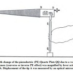
As shown in Figure 2, Curie brothers measured surface charges appearing on specially prepared PE crystals, on hanging a small weight from the crystal. Generated charge was measured by opening up of attached leaves of an electrometer. Tourmaline, quartz, topaz, cane sugar and Rochelle salt were used as their PE samples. For detecting the inverse PE effect (Figure 3), a thin and long quartz plate, QQ, was sandwiched between two tin foils. By applying a voltage to the tin foils, the quartz plate elongates or contracts according to the polarity of the applied voltage. To measure the very small displacement, they used a lever ABD. The displacement of the tip (A) of the long arm of the lever was measured with an optical microscope.
Figure 3. Length change of the piezoelectric (PE) Quartz Plate QQ due to a voltage applied across its thickness (converse or inverse PE effect) was magnified by lever action, to move the tip A. Displacement of the tip A was measured by an optical microscope.
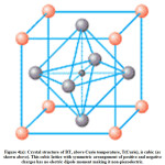
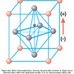
Using the example of piezoelectric effect in BaTiO3 (BT) in its tetragonal (orthorhombic) structure below T(Curie) ~120 °C, and no PE effect in its cubic perovskite structure above T(Curie) ~120 °C, Figure 4(a) & 4(b), one can confirm that non-centro-symmetry in crystal structure generates piezoelectricity.
Figure 4(a).Crystal structure of BT, above Curie temperature, T(Curie), is cubic (as shown above). This cubic lattice with symmetric arrangement of positive and negative charges has no electric dipole moment making it non-piezoelectric.
Figure 4(b). Below Curie temperature, T(Curie), the perovskite structure of Figure 4(a) is distorted with a shift of the small metal ion (like Ti or Zr, shown in deeper black) with respect to the plane of the negative O2-ions generating an electrical dipole moment. So, BT is piezoelectric and ferroelectric for T<T(Curie).
Centers of positive and negative charges being different at T < T(Curie), an applied electrical voltage will change their separation leading to dimension change or generation of force if the dimension change is externally resisted. This is inverse or converse effect. Direct effect can be similarly understood. In Figure 4(b), an applied force (causing dimension change) will move the centers of positive and negative charges, causing electrical charging of the sample faces (equivalent to generation of voltage).
A sample may be a single crystal (SXL) or polycrystalline, consisting of crystallites or grains. A piezoelectric grain or SXL usually consists of many PE domains.1,14,15 Domain is a region in which all unit cells are polarized in the same direction (Figure 5). So, each domain has its own polarization direction, as shown in LHS picture of Figure 6 (and in Figure 5 for only a few domains). Random orientation of these polar domains results in zero net polarization for the sample as depicted in RHS part of Figure 5, so that piezoelectricity does not show up. “Poling” or orienting all the domains to practically same polarization direction turns such a non-PE sample PE. In “poling”, a constant electric field (often at mediumly high temperature) is applied to “force” all the dipole moments to align in one direction (middle picture in Figure 6). Remanent polarization (RHS picture in Figure 6) after withdrawal of the applied field appears enough to keep the sample practically unidirectionally polarized and piezoelectric. Synthetic PE materials (like polycrystalline FE ceramics) with a much improved piezoelectric response are nowadays manufactured commercially for specific actuating or sensing applications. These are always “poled” samples. This has been a big step, from naturally occurring PE materials, for moving towards applications.
Figure 5. Adopted from 1991 book by Y Xu (DOI: https://doi.org/10.1016/C2009-0-12800-3.) A polycrystalline sample consists of crystallites or grains, defined here by thick lines. There are many domains inside each grain[19], as shown. Each domain has its own polarization direction (indicated by an arrow). Random orientation of polarizations of the domains in a sample, represented in the RHS picture, results in zero net polarization of the sample.
Figure 6. Adopted from reference.[19]A domain of Figure 5 is represented here only by an arrow, showing the polarization direction. Explanation of poling process, vide text.
Since, the electrical-to-mechanical and mechanical-to-electrical energy transfer in a PE material takes place in a complex 3-dimensional way, tensor equations govern these processes.1,2,14,15 It involves electric field and polarization, which are vectors, and elastic stress and strain which are second-order tensors. Piezoelectric coefficients in the equations link the variables, and provide quantitative measure of the performance of the PE material, as detailed in above references and many texts. For example, dmh are the piezoelectric strain coefficients representing strain in h-direction due to an electric field applied in m-direction. Jbaily and Yeung have explained that unlike in elastic compliances and dielectric permittivities, dmh is different from dhm.15
It is noted that dmh also gives the electrical displacement created in m-direction by a stress, applied in h-direction. Generation of electricity (electrical displacement) from a stress obtained from vibration or ocean waves generally use either d31 or d33 mode.15 Here, d31 means 3-1 or (z-axis)-(x-axis) coupling mode, implying application of the stress in a direction perpendicular to that of poling, along which PE voltage will be generated. Similarly, in d33 or 3-3 coupling mode, the applied stress and the poling of the piezoelectric material have the same direction.16 Ocean energy recovery by PE effect is still in the developing stage. Nations with vast ocean or sea front can investigate its commercial viability.
Defect Form of Cadmium Oxide with High Electrical Conductivity
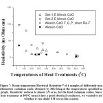
We observe cadmium oxide to assume different colors with different room temperature electrical conductivities on firing it (for 36 h in present tests) at different temperatures (Figure 7). A series of characterizations, proved thermally created non-stoichiometry defect.3,4,17,18 This must generate charge-carriers (found by us to be electrons for the samples subjected to Hall measurements), and, hence, extra electrical conductivity.
Figure 7. Room temperature Electrical Resistivity[3] of 4 samples of differently non-stoichiometric cadmium oxide, obtained by 36h firing at the temperatures specified in the graph. Resistivity reduces to almost 1/9 or so, for the fired cadmium oxides. Since, heat treatment at 800°C turns it into a good electrical conductor, we wanted to see whether it can shield EM waves like a metal.
Newer Polymeric Composites for Electromagnetic Shielding
Electromagnetic Interference (EMI) shields should better be flexible for easier and gapless coverage and also light. Metallic shields, the best for EMI shielding, loose on both counts to the 2nd generation EMI shielding materials based on polymers.6,19 On using a conducting polymer in pure or composite form, one still needs the addition of a binder polymer to get a flexible sheet. So, we tried a Si-based polymeric binder that is initially a liquid. It could be mixed with potential shielding powder/s and cured overnight to any desired shape.
Fe-Superconducting Compounds
The 1111 family of Fe-superconductors (RFeAsO with substitution, R = rare earth element), having tetragonal P4/nmm, ZrCuSiAs type structure, shows the maximum Tc ~ 56 K for Gd(1-x)ThxFeAsO at x = 0.20.[20] Here, we have chosen 122 family Fe-superconductors like Ba(Fe(1-x)Cox)2As2, x = 0.102 having Tc = 22.5 K.[8] Fe/Ni -based HTSCs being metallic, their fabrication into superconducting wires will be easier, with potential use in all high field magnets as needed in modern developments like fusion devices and accelerators. Our current work, mainly on radiation damage in Fe-superconductors, involves thin single crystal 122 samples to eliminate extra properties inevitable in polycrystalline and thin film samples.[21]
Experimental Results and Discussions
HT and Other Applications of Piezoelectric Materials
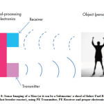
Piezoelectric imaging (using piezoelectric actuator/generator and sensor materials) find innumerable applications ranging from ultrasonography, fishing and underwater viewing (for navigation and warfare) to viewing, through high pressure molten metal coolant in Fast Breeder Reactors, of control and radioactive fuel rods.2,22 It is simple in principle. In Figure 8, reflected ultrasonic waves image the man. We have taken the freedom of showing the ultrasonic image itself as the Object (the man). Imaging by transmitted wave is also widely used.
Figure 8. Sonar Imaging of a Man (or it can be a Submarine/ a shoal of fishes/ Fuel Rods of a fast breeder reactor), using PE Transmitter, PE Receiver and proper electronics.
Common items like cell phones, diesel fuel injectors, acoustic guitar pickups, grill igniters, ultrasonic transducers, vibration sensors, certain printers, musical greeting cards and host of specialized and common applications utilize piezoelectric devices – often at lower cost and with better efficiency than other devices like eletro-magnetic devices. Applications discussed by us in 2015 will be largely skipped, but without affecting the completeness of present work.2 It will be useful to quote from the webpage of APC International about different applications of PE sensors, actuators and imaging devices.23
(a) “PE Engine Knock Sensors” detects detonation in petrol engines, and prevents explosion by a feed-back mechanism. This has reduced the safety margin of older cars without such sensors.
(b) “PE Pressure Sensors” is replacing strain gauges or displacement sensors.
(c) “Depth sounders and similar Sonar Equipments” rely extensively on piezoelectric sensors. It transmits and receives ultrasonic “pings” usually in 50-200k Hz range, with the advantage of high power density ~500 W, in a compact ~10 cm transducer.
(d) Replacement of older Diesel Fuel Injectors by “PE Diesel Fuel Injectors” mainly in last one decade or so. It now controls, with precise timing, the high pressure (~1800 bar) fuel at high rapidity rate (several times during a single power stroke) – reducing emission and noise, while increasing power and efficiency.
(e) “Solenoid Replacement” by PE Actuator, implying replacement of electromagnetic solenoids by “PE Solenoids” is a big step towards faster response, lower power consumption and fewer moving parts.
(f) “PE Micro Manipulators”, a kind of Solid State Motion, for fine movement in certain advanced investigations, correcting disturbances to mirrors / diffraction gratings or to earth-based telescope arrays or to spacecraft optics.
(g) “Ultrasonic Cleaning”
(h) “Ultrasonic Bonding” or “Ultrasonic Welding”
(i) “Piezoelectric Motors”, providing Solid State Motion, are more precise, compact and predictable. Unlike conventional motors, these can be designed to work in adverse environments with strong magnetic fields or at cryogenic temperatures.
(j) “PE Hammer” or “PE Drill” for heavy duty work.
(k) Deflection can be achieved in “Stripe Actuators”.[2] A Stripe Actuator is made by sandwiching together two strips of PE material in such a configuration (similar to a bimetallic strip) that an electric input causes one strip to expand while the other strip simultaneously contracts, causing a deflection. “Piezoelectric Linear Actuators” and “PE Bending Actuators” can now generate huge forces up to several kilo Newtons and large displacements up to several mm.[24]
(l) In line with the last entries, there are “Stack Actuators” or multiple piezoelectric elements may stacked to multiply the displacement achieved for a given voltage. These are used in proportioning valves, electrical relays, optical modulation, vibration dampening, and other applications demanding fast and/or precise control of movement.
(m) “Ultrasound Imaging” – “Medical” and “Industrial”. In addition to various medical detection it is facilitating minimally invasive surgical procedures.
(n) “Medical Ultrasonic Procedures” include use of focused ultrasonic waves to break up kidney stones or destroy malignant tissue. Also, the harmonic scalpel has allowed surgeons to simultaneously incise and coagulate tissue during a surgical procedure without the need for cauterization. This leads to less tissue damage, less blood loss, and faster healing.
(o) Inkjet-printer and dot-matrix-printer.[2,23]
(p) “Piezoelectric Speakers” found in cell phones, ear buds, sound-producing toys, musical greeting cards, musical balloons.
(q) “Piezoelectric Buzzers”, with lower fidelity than piezoelectric speakers, are louder. But they have a narrower frequency range.
(r) “Musical Instrument Pickups” — Many acoustic-electric stringed instruments have PE pickups to convert acoustic vibrations to electric signals.[23] Typically, a strip of PE material is placed between the instrument body and the structure that supports the strings. For instance, an acoustic-electric guitar usually houses its piezoelectric strip beneath the bridge and within the saddle. As the strings vibrate, the strip is agitated to generate an electric signal. Electrical pickups on violins, violas, and cellos use the same concept, but the PE pickup may be clamped to the bridge or integrated within the bridge — instead of being located between the bridge and the instrument body.
(s) “Microphones” — Various microphones (such as contact microphones for percussion instruments) use PE materials to convert sound to an electricity. These microphones generally possess high output impedances that must be matched when designing their respective pre-amplifiers.23
(t) “Piezoelectric Igniter”.
(u) “Electricity Generation through Piezoelectric Effect” is done by converting deflections or displacements (due to water waves, wind, dancing floor or engine vibrations) into electricity. Waste energy recovery will also cool the vibrating machine.
(v) “Under Liquid Sodium PE Viewing” of radioactive-fuel and control rods in a Fast Breeder Reactor (FBR) has been mentioned earlier, and detailed in our 2015 review.2
Point (v) above needs PE imaging and attention to keep FBR type nuclear reactors safe. U-235 from mined uranium is the most common fuel for nuclear power reactors that deliver green energy without any carbon footprint, while coal and oil fired power stations produce huge pollution and large C-footprint. Safe storing of Spent Fuel of the nuclear reactors is another problem, as the spent fuel still contains a lot of radio nuclides like U-238. Fast Breeder Reactor (FBR) can breed U-233 fuel from thorium (available worldwide and abundant in monazite sand in India) as well as fissile Pu-239 from U-238 in spent fuel (called nuclear waste), while producing electrical power.[2] So, FBR helps solve three problems (i) nuclear waste disposal through re-cycling of U-238, (ii) overcoming U-shortage by producing nuclear fuels and (iii) producing electricity. FBRs will continue to be strategically important to energy-starved India – till fusion energy is commercially viable. It appears that o-PNO (orthorhombic lead meta-niobate) has been used in Indian PFBR replacing PN used in FBTR (Fast Breeder Test Reactor) for ultrasonic imaging.2,25-28 We, Sahu and De (2014), also invented a process to eliminate risky and industrially difficult quenching step, and still get the orthorhombic FE phase.26
Point (u) is good for recovering waste energy, specially in low energy applications like cell phone charging. It is useful also for self-powering remote devices.
Further feeling of various practical applications of PE effect can be best obtained from a view of some items in US Patent and Trademark Office database:
- US Patent: 8,087,186: Piezoelectric-based toe-heaters for frostbite protection (Jahangir S. Rastegar, 3 January 2012): Innovatively placed PE devices in the shoes convert repeated squashing and stretching of the shoes into electrical energy that is used to warm the feet in freezing cold environments.
- US Patent: 20050127677: Roadway generating electrical power by incorporating piezoelectric materials (Jeffrey Luttrull, 16 June 2005): It harvests energy from vibrating roads or dancing floors.
- US Patent: 8,278,800: Multi-layer piezoelectric generator (Haim Abramovich et al, Innowattech, 2 October 2010): Details, with improvement, of generating electricity from vibrating roads.
- US Patent: 4,685,296: Ocean wave energy conversion using piezoelectric material members (Joseph R. Burns, 11 August 1987): PE device to produce electricity from the up-and-down movements of ocean waves.
- US Patent: 5,598,196: Piezoelectric ink jet print head and method of making (Hilarion Braun, Eastman Kodak, 28 January 1987): Widely used precise squirting of desired ink droplets due to electrical impulse induced dimension change of certain piezoelectric material in the ink tank of an inkjet printer.
- US Patent: US 20140128753 A1: Piezoelectric heart rate sensing for wearable devices or mobile devices (Michael Edward Smith Luna et al, 8 May 2014): An advanced PE instrument to monitor heart condition and send details to the designated mobile.
Minor applications of piezoelectricity are also many, with scope for new inventions. Flexible piezoelectric fibers, sewn into garments to charge mobiles or MP3 player, were developed (BBC News, 28-06-2011) at the University of Bolton. BBC News, 19-10-2005, revealed piezoelectric material based cochlear that can be implanted into ears to remove deafness in some cases.
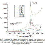
We will show here only three characterizations of these PE materials in Figures 9, 10 and 11. One is measurement of ε(i) = ε(imaginary) and ε(r) = ε(real), the imaginary and real parts of complex dielectric constant of the shielding material. Dielectric loss or loss tangent of present samples is defined as tan δ = ε(i) / ε(r). Cited references and texts document elaborately other characterizations like the measurement of piezoelectric coefficients d33 etc. Piezoelectric materials, based on barium titanate (BaTiO3 or BT) with T(Curie) ~ 120 °C, and those based on lead zirconate titanate (Pb(Zr,Ti)O3 or PZT) with T(Curie) ~ 370 °C have served us well for most of industrial, medical and consumer applications, generally involving room or near room temperature applications. Desirable piezoelectric parameters of PZT favored its wide applications. However, a few new and important applications, in automobile and rocket exhausts, in some engines and gadgets, and inside high pressure molten metal in Fast Breeder Reactors (FBRs) involve high temperatures (HTs), higher than or nearing the Curie temperature of even PZT. Here, PbNb2O6 (PNO), for which we found somewhat higher T(Curie) ~573 °C (Figure 9) than usually reported, and newer PE materials come in.2,25-28 While ferroelectric PE materials are in focus, there are some useful piezoelectric materials that are not ferroelectric. For non- ferroelectric PE materials, melting temperature roughly represents the upper limit of their piezoelectricity.
Figure 9. Variation of the real part (ε′) of the dielectric constant with temperature for various measuring frequencies (20Hz to 5.5 MHz) for orthorhombic PbNb2O6. The peak corresponds to Curie Temperature, T(Curie), below which the sample is piezoelectric and ferroelectric.[2]
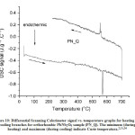
Figure 10. Differential Scanning Calorimeter signal vs. temperature graphs for heating and cooling branches for orthorhombic PbNb2O6 sample (PN_Q). The minimum (during heating) and maximum (during cooling) indicate Curie temperature[2,26].
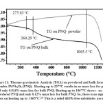
Figure 11. Thermo-gravimetric Analysis (TGA)[26] on powdered and bulk forms of orthorhombic PbNb2O6 (PNQ). Heating up to 257°C results in no mass loss for powdered PNQ and only 0.014% mass loss for bulk PNQ. Heating up to 1067°C shows – no mass loss for powdered PNQ and only 0.12% mass loss for bulk PNQ. So, there is no significant Pb-loss on heating up to 1065°C.[2] This is a relief till Pb-free substitutes are ready.
Presently, langasite (LGS), LiNbO3 (LN), AlN, YCa4O(BO3)3 i.e. (YCOB) and orthorhombic PbNb2O6 appear to be the most widely used piezoelectric materials for ultrahigh temperature applications due to their stable performance at ultrahigh temperatures. HT YCOB devices in particular, including accelerometers, ultrasound transducers, and acoustic emission sensors show a highly steady and reliable operation even at temperatures over 1000 °C. In general, piezoelectric actuators and miniature motors are yet to reach such a high temperature.[2] Only recently, a high temperature monolithic compression-mode piezoelectric accelerometer was fabricated using YCOB single crystals. It was tested successfully as a function of temperature up to 1000 °C and in the frequency range 100–600 Hz. The prototype accelerometer showed a sensitivity of 2.4 (0.4) pC/g, across the measured temperature and frequency range, indicating a low temperature coefficient. Furthermore, the sensor exhibited good stability over an extended dwell time at 900 °C. So, YCOB i.e. YCa4O(BO3)3 piezoelectric accelerometers are promising candidates for high temperature sensing applications.
PE devices are being developed to monitor and optimize the propulsion systems for operations at temperatures up to 1000°C or even 1250 °C to enable safer, more fuel-efficient and more reliable vehicles, rockets and missiles.2,29 This includes measuring flow rate and monitoring of exhaust composition to check pollution. A particular chemical coating that absorbs a particular gas, is given on a quartz crystal oscillator. Gas absorption increases the oscillator mass causing a detectable change of the oscillation frequency. This way gases like SO2, CO, CO2, O2 and hydrocarbons in the exhaust can be identified and concentration estimated. Compared to commercial strain gauges and optical fibre sensors, PE sensors already reach higher temperature (>600 °C), higher accuracy, faster response and ease of integration.[40] Advantages of PE injection of diesel in automobile engines has already been discussed.
A large number of ferroelectric materials (vide Tables 1-3 of reference[2]) are candidates for high temperature piezoelectric applications:
(a) polycrystalline ceramics with perovskite and tungsten bronze structures, including PNO,
(b) bismuth layer structures (bismuth layer structured ferroelectric, BLSF, or Aurivillius componds)
(c) double perovskite layer structures (double PLSs).
(d) Single crystals like LiNbO3 (LN) and LiTaO3 (LT), with corundum structures that are ferroelectric materials, with Curie temperatures of 1150 °C and 720 °C, respectively.
More details of few potential high temperature PE materials will be interesting:
Advantage of piezoelectric sensors and actuators in practical applications is now extending to modern high temperature (HT) applications in the aerospace, aircraft, automotive and energy industries for achieving improved fuel efficiency, reduced emissions, decreased maintenance cycles and decreased failures. More information can obtained from industries like Dytran Instruments Inc., by reviewing their websites <www.dytran.com>. They offer, among many instruments, (i) Smallest Accelerometer (20 gm), capable of operation up to 650 °C, (ii) exhaust manifold testing and (iii) engine vibration monitoring meant for testing Turbines, Rockets and Automobiles. Higher temperature PE accelerometers are also available.
Table 1: A comparison of some HT PE materials.[2] Usage temperatures# have been suggested on basis of a standard of 1 MΩ.cm resistivity for comparison purpose. Here, standard abbreviations: LN for LiNbO3, LGS for langasite, YCOB for YCa4O(BO3)3 & also GdCOB, have been used. Lower resistivity materials (like LN) can often be used for a short period and in the high frequency range, at somewhat higher temperatures (~ 1000 °C for LN).
|
Material
|
GaPO4
|
LN
|
LGS
|
YCOB
|
GdCOB
|
|
Tmax (°C) (phase transition or melt)
|
970
|
1150
|
1470
|
1510
|
1470
|
|
Tuse (°C) (suggested usage temp) #
|
700
|
600
|
800
|
~1250
|
<1200
|
|
Temperature limited by
|
Phase transition & attenuation
|
Resistivity
|
Resistivity
|
Resistivity
|
Resistivity
|
|
Mechanical quality factor
|
10,000
|
2000
|
15000
|
9000
|
5000
|
|
Dielectric loss
|
0.15
|
5.5
|
0.5–0.2
|
0.3–0.1
|
0.3–0.2
|
|
Dielectric permittivity variation (%)
|
5
|
~ 40
|
25–15
|
15–10
|
10–9
|
|
Resistivity (MΩ∙cm)
|
23
|
0.66
|
2 to 8
|
10 to 200
|
4 to 30
|
There are many suppliers, like Mitsubishi Materials Co. Ltd., Japan, of piezoelectric materials (like LiNbO3 single crystals of different orientations and LGS, La3Ga5SiO14, crystals).[29] The recent mandate of the European Union to develop, through METCO, the metrological infrastructure and facilities within Europe for the traceable metrology of piezoelectric, ferroelectric, thermal, and electrocaloric properties at high temperatures and applied electric fields, highlights the importance of this research area.
Polymeric Composites for Electromagnetic Shielding
Ever growing use electrical and electronic devices in industrial, commercial, R & D and home applications has resulted in many-fold increase in generation of EM waves. This is increasing unwanted EM Interference (EMI) to other devices and to living beings to the extent of suspectedly causing cancer. Polymeric composites that we fabricated include EMI Shielding materials and Radar Absorption Materials (RAMs). Following two parameters quantitatively describe reflection, absorption and transmission of such electromagnetic waves in materials.[5,6,25]
(i) Shielding Effectiveness (or its negative, called Shielding Efficiency), and
(ii) Reflection Effectiveness (or its negative, called Reflection Efficiency).
Figure 12 is an overview of three main types of the novel polymer-solid composites, presently developed using a Polymeric Binder or PB, namely Silicone sealant 732 or Silicone sealant 734 from Dow Corning, as the polymer. This PB, purchased in tubes, is a thick liquid. On uniformly mixing it with one or more solid powders and allowing overnight curing, flexible Si-rubber composites in sheet form (the EM shield) could be obtained. Vector Network Analyzer (VNA) technique, a widely used technique of measuring microwave reflection and transmission[6], has been utilized here. By measuring:
Pin, EM power incident on the shield,
Preflec, EM power reflected by the shield, and
Pout, EM power transmitted through the shield,
in the VNA, one can know, Pabsorb = EM power absorbed in the shield.
The 2-port network parameters S12 = S21 (for transmission) and S11 (for reflection) are related to transmittance and reflectance:
T = Transmittance = Pout / Pin = |S12|2 and R = Reflectance = Prefl / Pin = |S11|2.
Since R = reflected fraction of EM wave intensity and T = transmitted fraction, A = absorbed fraction, can be found from the equality: R+A+T = 1.
Absorbed power = (Pin – Pout – Prefl).
For quantitative estimate of total shielding one defines:
SE = Shielding Effectiveness in dB unit = 10 log (Pout / Pin).
Since Pout < Pin, SE will be a negative quantity. A large negative value of Shielding Effectiveness will, therefore, indicate high shielding. To avoid dealing with this negative quantity, many authors[4] define a new parameter:
Shielding Efficiency = – 10 log (Pout / Pin) in dB = 10 log (Pin/Pout) in dB, which has higher positive value (larger Pin/Pout), for materials that shield more.
Similarly, 10 log (Prefl / Pin) in dB = Reflection Effectiveness = RE, is a negative quantity, and Shielding Efficiency = – 10 log (Prefl / Pin) in dB. These arise from reflection. However, the terminology in certain treatise is often different from what we present here.
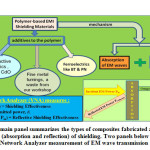
Figure 12. The main panel summarizes the types of composites fabricated and the expected mechanisms (absorption and reflection) of shielding. Two panels below schematically explain Vector Network Analyzer measurement of EM wave transmission and reflection.[6]
Three main types of polymer-solid composites indicated in Figure 12 have been extended to their mixtures in search of better results. A full list of our composite samples is given in Table 3 of reference[6]. Weighed amounts of this sealant (PB) and components have been mechanically mixed for 20 to 40 minutes into a dough-like mixture, and then pressed between a Teflon plate and a glass plate into a sheet of approximately the desired thickness. An important reason for choosing the Dow Corning Silicone sealant is that the composite sheet cured overnight into a flexible cloth-like rubber-sheet. Chemical inertness is another advantage of this polymeric binder. Unexpected shielding activity of the sealant has been noticed in sheets without any additive(s).
For situations30 with negligible magnetic interaction and low internal multiple reflections correction term, the decibel value of EM Shielding Effectiveness (SE or SEtotal) is simplified to:
SE = SEtotal = SEreflection + SEabsorption
For 700 MHz to 3 GHz VNA measurements, based on coaxial holder, annular samples (or circular samples with central hole) have been prepared by a newly devised Double Plunger[6]. Rectangular wave guide system is used in VNA frequency ranges covering 8 to 40 GHz. This needs rectangular samples – in four specified sizes for the four above-mentioned frequency ranges. Present VNA gives the variations of 10 log (Pout / Pin) = Shielding Effectiveness in dB unit = SE, related to S12, and 10log (Prefl / Pin) in dB = Reflection Effectiveness = RE, related to S11, with frequency graphically, with digital data for selected representative points.
Some Selected Highlights of Polymeric Composites for EMI Shielding
Success has been achieved for the newly used self-curing polymeric binder to prepare a variety of flexible cloth-like composites (numbering 52), and measure SE and RE over the wide range 700 MHz to 40 GHz (Figures 13 & 14 for example).
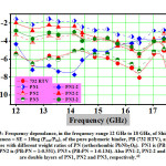
Figure 13.Frequency dependance, in the frequency range 12 GHz to 18 GHz, of Shielding Effectiveness = SE = 10log (Pout/Pin), of the pure polymeric binder, PB (732 RTV), and its composites with different weight ratios of PN (orthorhombic PbNb2O6). PN1 is (PB:PN = 1:0.952). PN2 is (PB:PN = 1:0.551). PN3 s (PB:PN = 1:0.134). Also PN1-2, PN2-2 and PN3-2 are double layers of PN1, PN2 and PN3, respectively.[6]
Figure 14. Variation of shielding effectiveness, 10 log (Pout/Pin), with frequency, of 6 composites our Polymeric Binder (PB) with one or more of CdO-800, BaTiO3 (BT), Brass turnings (Brass) and Copper turnings (Cu) in compositions as listed in the Figure with Sample Name and Symbol. This is in the frequency range 26 GHz to 40 GHz.[6]
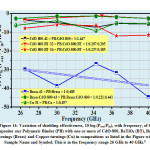
Brass and copper turnings, which can be obtained practically free from mechanical workshops, were cleaned and sieved through a 1mm X 1mm net, before making brass and copper composites (Figure 14). Its success paves the way for reducing cost.
Figure 13 shows the new but welcome feature of two transmission minima[6]: SE = -10.68 dB at 17.69 GHz and SE = – 8.08 dB at 16.5 GHz for non-conducting 732 RTV, chosen only as the polymeric binder (PB). It may be helpful towards RAM applications. Composites show these minima in a diluted way. Here, doubling of layer (like making PN1 into PN1-2) decreases transmission (except for end-zone 17.7 to 18 GHz) – but only for the highest PN-content polymer composite (PN1, composition: PB:PN = 1:0.952),where PN contribution is likely to dominate. PN or o-PNO appears to be an EM wave absorbing material. For lower o-PNO containing composites, PN2 (PB:PN = 1:0.551) and PN3 (PB:PN = 1:0.134), where added PN or o-PNO is less dominating, more power is seen to be transmitted i.e. absorption decreases on going to double layer (PN2-1 to PN2-2). So, it is felt that possible contributions to electromagnetic shielding (i.e. to EM wave reflection and absorption) from factors like interface and microstructure need to be investigated more seriously.
Measured SE = – 44.82 dB (Figure 14) for PB/Brass (Brass 41) at 39.997 GHz,[5] and SE = -32.83 dB for PB/Cu (Cu 51) at 10.380 GHz, in Figure 9 of Sahu and De,[6] are already high, although no optimization steps have yet been carried out. Composites / multicomposites with BaTiO3 or BT with T(Curie) = 124°C have also been studied.[6] EMI SE of -29.71 dB at 9.901 GHz for the non-metallic composite PB/CdO-800/BT (CdO-800 BT 34) is very satisfying. Shields prepared from metal turnings have performed well.
Reflection effectiveness, 10 log (Prefl / Pin), of polymeric composites involving PN, BT and metal turnings (over ~26 to 40 GHz), is depicted in Figure 15.
Figure 15. Variation[6] of reflection effectiveness, 10 log (Prefl/Pin), with frequency, of 6 composites our Polymeric Binder (PB) with one or more of CdO-800, BaTiO3 (BT), Brass turnings (Brass) and Copper turnings (Cu) in compositions, listed in the Figure with Sample Name and Symbol. This is in the frequency range 26 GHz to 40 GHz.
It is further noted, that for conductive composites (CdO_800), reflection part increases (~ 10.64%) and absorption part remains practically unchanged (only ~ 0.43% change), on increasing thickness (CdO_800 33 sample, single to double layer change), to show reflection to be the dominating mechanism. For dielectric composites (PN35), on the other hand, reflection part changes little (~ 2.42% change only) and absorption part increases significantly (~ 7.46%), on increasing dielectric powder (PN) wt.% from 13.4 to 55.1. Transmission is much less in X- band than in UHF band implying better EMI shielding. For example, PN352 sample transmits 24.4% for single layer and ~ 15.7% for double layer at 11.256 GHz (X-band), whereas it has ~ 71.1% transmission at 3 GHz (UHF band). Also, absorption increases from ~ 17.5% (at 3 GHz, UHF) to ~ 26.2% (at 11.256 GHz, X-band). PN samples shield better than BT or BT_CdO samples in low frequency range (700 MHz to 3 GHz). Copper composite polymer samples act as better shielding materials (~ 0.05% transmitted at 10.3822 GHz) than brass composite polymer sample (1.01% transmitted at 10.3822 GHz), in 8 to ~ 10.83 GHz range. But, brass composite polymer sample shows better shielding (0.18% transmission at 11.600 GHz) performance than Cu composite polymer sample (1.12% at 11.600 GHz) above ~ 10.83 GHz – up to the highest frequency studied here (12 GHz). Low transmission i.e. good EMI shielding by these workshop waste materials (copper and brass turnings) has been possible by our fabrication of cloth-like polymeric composites with these materials, opening up a lower cost substitute for the widely used metal sheets and wire-meshes. The fabrication needs to be further perfected for optimum EMI shielding.
Polymeric composite PN3 (PB:PN = 1:0.134), involving the Polymeric Binder (PB) and ferroelectric o-PbNb2O6 (PN) is a good Absorbing Material at around 19.1 GHz, as reflection as well as transmission has been measured, to be low. PN3 has large absorption also around 22.04 GHz.6 These provide base for developing RAM or Radar Absorbing Materials.
Polymeric composites like Cu-51 (PB:Cu = 1:0.4969) and Brass-41 (PB:Brass = 1:0.4854) have been made from mechanical workshop waste of copper and brass turnings. Cu-51 shows low transmission of -28.03 dB at 12 GHz (in Figure 9) and similar or lower transmission down to ~ 8.4 GHz (Figure 9).2 Similarly, brass composite sample Brass-41 (PB:Brass = 1:0.4854) is a low transmittance or EM shielding material, transmitting only ~ 0.21% to ~ 0.003% (- ~ 26.87 dB to ~ – 44.68 dB) in 26 to 40 GHz frequency range, as shown in Figure 11.[3] So, use of waste copper and brass turnings instead of metal powders is providing good EM shielding at much lower cost. Adding ferroelectric powder PN3 in the polymeric binder (PB:PN = 1:0.134) induces EM wave absorption. Discovery of RAM-like high EM wave absorption in the 732 RTV polymeric binders itself is another important finding of this work.
More work remains to be done than what have been done, for understanding and fruitful applications.
Characterization of Non-Stoichiometry in II-VI (Cd-O) Samples and Their Novel Properties
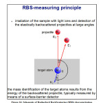
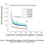
It has been known for decades and even recorded in standard chemistry texts (F.A. Cotton and G. Wilkinson (Wiley), and H. Remy (Elsevier)) that cadmium oxide, prepared by different techniques, show different colors ranging from black to gray and golden. But it was never seriously investigated before we started this work around 1996.3,4,17,31,32 We wanted to investigate in more details, also because CdO is a II-VI compound, potentially important as a semiconducting material. Next, we found that prolonged heat treatment (decided to be 36 h) at different temperatures give at room temperature – different colors, and more importantly, different electrical conductivity. Firing at 800 °C or so produced black Cd-O. Clearest indication of the real difference of the differently fired samples came from our Rutherford backscattering experiment using 3.05 MeV alpha-beam at the pelletron facility of IOP, Bhubaneswar, India (Figure 16).4 Measured energy of the backscattered projectile (here, alpha-particle) gives the mass of the target (sample) atom that backscattered it (say Cd). The intensity of the backscattered alphas at that energy corresponds to atomic percent of the scattering atom (here, Cd, giving Cd step in the intensity vs. energy plot, Figure 17).3,4 The energy of 3.05 MeV of the projectile alpha beam was chosen to give the resonant scattering peak of O-atoms in the samples, in addition to the step for Cd. Larger RBS step for Cd will imply more Cd in the sample (Figure 17). In these characterizations, relative compositions rather than absolute compositions have been determined as no standard Cd-O have been available for calibration. Our RBS also showed that 700 °C firing of ZnO_400 increased relative Zn% implying O-loss.
Figure 16. Schematic of Rutherford BackScattering (RBS) characterization.
Figure 17. Different RBS step heights for Cd in CdO samples after 36 h firing at temperatures indicated in °C in sample names.
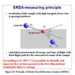
Cd-O composition was investigated also by Elastic Recoil Detection Analysis (Figure 18-20),3 with TOF (Time Of Flight) detection of recoil or scattered atoms of the sample, at HMI, Berlin, in collaboration with J. Roehrich and W Bohne. Coincident measurement of energy E of each recoil atom and its velocity v (from flight time over a known distance) gave mass of the recoil atom using relation E = (1/2)Mv2. Deducting composition from this data involved many simplifying assumptions, and values in Figure 19 are not the absolute values.
Figure 18. Principle of Elastic Recoil Detection Analysis (ERDA).
Figure 19.TOF-ERDA raw data on our 1175°C fired Mg-O, scatterplot of recoil energy vs. time of flight – different traces for different elements. Large intensity (red) of Mg and O compared to impurities or surface contaminations can be noted. It is not ideal for presently used pellet sample that can have trapped moisture etc. [3]
Figure 20. Cd:O for “CdO” from ERDA after 36 h firing at different temperatures.[3]
Exact composition could not be obtained by any of the techniques. Atomic Absorption Spectroscopy (AAS) determines bulk composition.3,17 Other techniques probe down to the depth reached by the probing fast particle or ray. Still, composition approximately estimated by AAS and X-ray Photoelectron Spectroscopy (XPS), are quoted below. Apparent fall or near constancy of “estimated” Cd-content on moderate heating and rise in Cd-content or O-loss at higher temperatures towards 800 °C appear to be suggested by all the techniques, although details differ due inherent special factors of different techniques and compromises in our data analysis. These pellet samples contain a lot of absorbed and adsorbed moisture, different gases and dirt. These are removed by heat up to moderate temperatures increasing fraction of detected Cd in the sample. By not taking this partly known factor into consideration one can wrongly conclude fall of Cd fraction in “CdO compound” up to moderate temperatures. Real fall of Cd-fraction in “CdO compound” would have to involve O-intake by the O-rich sample at this low temperature, while O-loss is confirmed, at least at higher temperatures.
Table 2: Rough estimate of Cd at.% in differently fired (36 h) cadmium oxide from XPS and AAS techniques.
|
Firing Temperature °C
|
30
|
237
|
270
|
375
|
382
|
400
|
800
|
|
Cd at% from XPS* (surface data, No std.)
|
52.6
|
59.2
|
53.1
|
|
62.11
|
|
61.9
|
|
Cd at% from Atomic Absorption Spectro.#
|
32 .7
|
32 .7
|
25.8
|
36.5
|
36.3
|
35.7
|
45.3
|
Thermogravimetry (Figure 21), shows that as-supplied CdO loses weight or mass basically at two temperatures, as marked in the Figure. Differential Scanning Calorimetry (DSC) records (Figure 22) heat absorbed by the sample (endothermic process) or heat evolved by the sample (exothermic process) for upward or downward temperature scanning of the sample.[3] Here, taking out atoms must be endothermic, the two dips or minima in our DSC. These endothermic dips are at the 2 major steps of mass loss in TGA – a satisfying agreement. Heating of cadmium oxide should, therefore, involve more and more O-loss, basically at the indicated temperatures. Midway between these endothermic dips, one sees a large exothermic peak that needs to be explained. The O-loss from random positions at the lower temperature endotherm must have left the sample rather disordered. So, on further increase of temperature a re-arrangement of Cd and O atoms into a lower potential energy structure may have taken place as supported by evolution of heat. So, higher temperature of the higher temperature endotherm is needed to eject more atoms, as evidenced from TGA, from the structure.
Figure 21. Thermogravimetry of as-supplied cadmium oxide in air for heating at the rate of 1 ºC /min.[3]
Figure 22: Differential Scanning Calorimetry (DSC) of as-supplied cadmium oxide in air for heating rate of 1 ºC /min.[13,46]
Knowing and understanding non-stoichiometry in II-VI compounds like CdO, ZnO and MgO is essential before undertaking their doping to make p type or n type semiconductors.
Fe-HTSC – Characterization and Application Potentials
The Fe-based HTSCs fall in following 4 families, identified by their general formulae and the high temperature crystallographic structures:
(1) The 1111 family (RFeAsO with substitution, R = rare earth element), having tetragonal P4/nmm, ZrCuSiAs type structure, showing maximum Tc ~ 56 K for Gd(1-x)ThxFeAsO at x = 0.20,33
(2) 122 family (AE1Fe2As2, mostly with substitution, AE = an alkaline earth element like Ba, for Ba122), having tetragonal I4/mmm, ThCr2Si2type structure, showing maximum Tc = 38 K for Ba(1-x)KxFe2As2, x=0.4,34
(3) The 111 family (LiFeAs and NaFeAs, with or without substitution) having a tetragonal P4/nmm, PbFCl type structure, showing maximum Tc = 18 K in LiFe1:03As,35
(4) The 11 family (FeSe(1-x)Tex, non-stoichiometric or with substitution) having tetragonal P4/nmm, α-PbO type structure, showing maximum Tc =16 K in FeSe0.8S0.2.13,36
On lowering the temperature below a certain temperature (Ts), the metallic parent compound shows a tetragonal-to-orthorhombic structural change: to Cmma for the 1111 family, to Fmmm for the 122 family, to Cmma for the 111 family, and to structures like Pnmm for the 11 family.[20,21,37-39] Various mechanisms of superconductivity involving magnetic interactions have been suggested for these Fe-based superconductors.13
Now we note that the high temperature structure for all the 4 families is tetragonal. More important is the fact that they all contain Fe-As or Fe-Te/Se layers in tetrahedral coordination, and superconductivity originates from these layers. For these reasons, doped BeFe2As2 or 122 superconductors can roughly represent all the four families. It has the relative ease of making its SXL, as our advantage for working on Ba(Fe(1-x)Cox)2As2. Still, above outline is included to introduce all the Fe-HTSCs.8,21,40
A 5th structure with FePn-planes,where Pn= Pnictide, to join this superconducting set of materials is the so-called 21311 (sometimes called the 42622) structure.[43] The first member Sr2ScO3FeP found by Ogino et al. in 2009 showed Tc =17 K. The 6th and most recent FePn/Ch structure with superconductivity (Tc = 32 K) is an ordered defect alteration of the 122 or BaFe2As2 structure (called the ‘‘122*’’ structure herein), written as A0:8Fe1:6Se2.43
High values of Jc (superconducting critical current density), Tc (superconducting critical temperature) and Hc2 (superconducting upper critical field) qualify likely performance of a superconducting material as the wire or cable in a superconducting magnet. Both Cu-O based HTSCs like YBa2Cu3O(7-δ) and Fe-As or Fe-TE/Se based HTSC 7677like doped-Ba122 are good with respect to Jc and Hc2. Although Tc of doped-Ba122 is little lower, its metallic nature offers easier fabricability into a cable and it is more isotropic than Cu-O based HTSCs.[17,43] Co-doped Ba 122 turned out to be best for making high current conductors. Intrinsic Jc of BaFe1.84Co0.16As2 is already within 1 order of magnitude of best “old” superconductors with similar Tc (Nb3Sn), as discussed by M Brian Maple, UC (San Diego). For using the Fe-superconducting Tapes in large magnets in radiation environments, radiation damage experiments are important.27,55 Suitable irradiation induced defects can also increase critical current density, as discussed next from a recent publication.44
In type II practical superconductors like Cu-O HTSCs, critical current density (loss-less electrical current density), is increased by increasing vortex pinning centers in the superconductor so that the flux lattice is pinned by these centers.[15-17] Columnar defects generated by swift heavy ions have produced best pinning centers in Cu-O HTSCs. Fang et al. have irradiated, along c-axis of the crystal, two SmFeAsO0.8F0.15 single crystals with 1.4 GeV Pb-ions to doses of N= 2 × 10¹¹ ions cm−2 (sample no. 1, & corresponding to nominal dose-matching field of BΦ= 4 T) and 5 × 10¹¹ ions cm−2 (sample no. 2, dose-matching field of BΦ= 9.5 T). Here, BΦ=NΦ0, where Φ0=2.07 × 10¹⁵ Tm2.44 Heavy Pb ion creats amorphous tracks or columnar defects, only ~2–5 tracks per 1000 unit cells.
Like earlier-mentioned Co-doped Ba122, Ba0.6K0.4Fe2As2 has been quoted to show a nearly field-independent and high critical current density of Jc= 5 MA cm−2 at 5 K and H~7 T, comparable to that of best YBa2Cu3O7-δ-coated conductors under similar conditions. However, the relatively low Tc of Co-doped (23 K) and K-doped (38 K) samples was the disadvantage. High Tc > 50 K in FeAs-1111 compounds, like SmFeAsO1−xFx, plus its Jc approaching 1–2 MA cm−2 in as-grown SmFeAsO1−xFx crystals and films at 5 K and self-field appeared attractive.45 Disadvantage was the layered structure of SmFeAsO1−xFx, shown in Figure 23(a), leading to high anisotropy, γ~8, higher than YBCO. This suppresses the irreversibility field, limiting applications at high fields and high temperature. Fang et al. mitigated these disadvantages, by generating above-mentioned nano-scale columnar defects in optimally doped SmFeAsO0.8F0.15 crystals.44 That brings many benefits (Figure 24). They incorporated a low density of columnar defects into pristine SmFeAsO0.8F0.15 crystals by using high-energy, heavy-ion irradiation along the c-axis. The induced columnar defects produce very high critical current density, as shown in Figure 24(c), without degradation of the transition temperature, vide Figure 23(e). The enhanced critical current of Jc (5 K, 0 T) ≈ 20 MA.cm−2 corresponds to ~20% of the depairing current density. Interestingly, the radiation also reduced the superconducting anisotropy from 8 to 4. This can be qualitatively explained in the framework of anisotropic electron scattering by columnar defects.
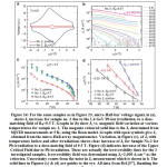
Figure-23: GeV Pb-ion irradiation[42] on SmFeAsO1−xFx crystal, with layered structure(a), along c-axis of the crystal, produced nano-scale columnar defects (b). Picture (c) is the image of the so-called sample number 1 placed on top of a micro-Hall array magnetometer. Pictures (f) and (g) are magneto-optical images of the magnetic flux tube in the sample in increasing and decreasing applied magnetic fields. Graphs (d) and (e), magnetization measurement results of sample nos. 1 & 2 before and after irradiation show practically undiminished Tc. The scale bars in (c) and (f) indicate 100 μm. Next Figure, Figure 24(a), will show huge increase of critical current density (Jc). Fine adjustment of the experiment achived this increase of Jc without Tc degradation. All data from Ref.[42], thanking the authors.
Figure 24. For the same samples as in Figure 23, micro-Hall-bar voltage signal, in (a), shows Jc increase for sample no. 2 due to the 1.4 GeV Pb ion irradiation, to a dose-matching field of BΦ=9.5 T. Graphs in (b) show Jc vs. magnetic field variation at various temperatures for sample no. 2. The magenta coloured solid line is the Jc determined from SQUID measurements at 5 K, using the Bean model. Graphs with open symbols give Jc obtained from the micro-Hall-array magnetometer. Variation, in Figure (c), of Jc with temperature before and after irradiations shows clear increase of Jc for Sample No.2 for Pb-irradiation to a dose-matchig field of 9.5 T. Figure (d) indicates increase of the Upper Critical Field due to Pb-irradiation. These are actually the irreversibility lines for the 3 investigated samples. Irreversibility field was determined using Jc=2,000 A.cm−2 as the criterion. Uncertainty comes from the noise in Jc measurement which is shown in b. The solid lines in Figures (c) & (d) are guides to the eye. All data from Ref.[42], thanking the authors.
A reduction of the anisotropy after heavy-ion irradiation with virtually unchanged Tc was also observed in 122-compounds. The anisotropy of Ba0.6K0.4Fe2As2 is reduced from 2.5 to 2.1 after 1.4 GeV Pb-ion irradiation to a dose of BΦ=21 T; heavy-ion-irradiated SrFe2(As1−xPx)2 shows an anisotropy change from 1.6–1.5 to 1.2–1.3. The comparatively small reduction of anisotropy in the FeAs-122 materials can be attributed to the initial low anisotropy and the discontinuous morphology of the damage tracks. Similar phenomena is expected in high-Tc cuprates, MgB2 and other anisotropic superconductors. Very limited attention has been paid to the reduction of the superconducting anisotropy due to correlated defects in these materials. In the case of cuprates, any change of Hc2 is convoluted with a reduction of Tc, whereas the high conductivity of MgB2 and of most conventional superconductors has prevented the creation of columnar defects with heavy-ion irradiation. For Fe-based superconductors, their semimetal property and weak gap anisotropy enable one to tune the anisotropy via heavy-ion irradiation. Other poor-metallic and fully gapped type II superconductors can be expected to follow present predictions and demonstrate tailored anisotropy. This general phenomenon is important for the application of new superconducting materials.
The low anisotropy, high Jc and high Tc of optimal-doped SmFeAsO1−xFx indicated that it was then the best Fe-based superconductor for practical applications. SmFeAsO1−x Fx thin film synthesis has progressed well. Further improvement of the performance of these films can be expected on introducing columnar-type defects. Self-assembled columnar defects, possible in Cu-O HTSCs can be tried in Fe-HTSC films.
Having discussed few of yet the best Fe-HTSCs for making high current superconducting films and wires, an outline of making such wires will be appropriate.45 Techniques like pulsed laser deposition (PLD) onto room temperature LaAlO3 and MgO substrates have been used successfully and rather widely to deposit thick films for high current conduction with zero resistance. Using powder-in-tube or (PIT) method, Gao et al. prepared in 2008, SmFeAsO0:65F0:35 wires by filling 8 mm diameter Ta-tube of, 1 mm wall thickness, with stoichiometric amounts of the constituent reactant powders, swaging down the tube to 2.25 m diameter and reacting at 1170ºC C for 45 h.58 The resulting wire had Tc(onset) of ~ 52 K, a global critical current density of 3900 A/cm2 at 5 K, and WHH formula Hc2(T~ 0) >100 T. Using the PIT method, Ozaki et al. (2011) prepared single core and 7 core FeTexSe(1-x) wires, with Tc(onset) ~ 11 K, and Jc (4 K) ~ 200 A/cm2. As expected, critical current density Jc in single crystals have much higher values in above-mentioned wires. Ma et al. (2009) also discussed the PIT process, with Nb or Fe tubes in addition to Ta. Wang et al. (2010) prepared Sr0.6K0.4Fe2As2, Tc ~ 34 K, SC tape with Ag sheathing to reach Jc (4.2 K) ~ 1200 A/cm2.
Concluding Summary
As outlined elaborately, continuing development of specialized piezoelectric materials and intelligently designed devices have led to
(i) varied, precise, fast and economical detection or sensing, of pressure or movement through direct piezoelectric effect – with control through added feed-back mechanism,
(ii) varied, precise, fast and economical generation of force or motion (from micromanipulator to hammer) through inverse or converse piezoelectric effect, and
(iii) varied, precise and fast imaging – through different ultrasonography scanning – either inside human body and liquid-metal-filled fast breeder reactor or outside under the sea of fish shoals or submarines.
Items in (i) and (ii) are, in most aspects, superior to electro-magnetic or similar devices, justifying their nicknames: electronic muscle and solenoid replacement. These are usually more economical than electromagnetic devices, that often involve bulky moving parts. Latter consumes more electricity and require more frequent replacements. Industries need to notice latest of successful applications of piezoelectricity, and more importantly potential applications that can be profitably exploited. Here, earlier discussion of piezoelectric sensing of fuel and exhaust gases in automobiles, aircrafts, rockets and missiles and necessary control may be recalled. Even chemicals in the exhaust are detected by frequency change due mass change of an implanted piezoelectric oscillator due absorption of the targeted gas by the target-specific coating given on the piezoelectric oscillator. These advances have led to great improvements in automobile engine performance.
There is harmful Electromagnetic Interference (EMI) to humans and sensitive instruments in certain range of the Electromagnetic Spectrum (Table 1 of Reference42) like the microwave range. EMI Shielding of either the source or to-be-protected item is best done by a suitable gapless metal sheet shielding. Difficulty of making the metal shield gapless and its higher weight with respect to a flexible polymer-based shield have moved the world towards 2nd generation EMI Shielding by Polymeric Materials. Others using conducing polymer with solid particle inclusion, have to usually add a binder-polymer or adhesive material. Here, composites of a polymeric binder only with EM wave reflecting particles (of a metal or a conducting oxide) or with EM wave absorbing particles (ferroelectric or dielectric) or their mixture have been developed as flexible sheets and their EM Shielding Effectiveness (SE or SEtotal) and Reflection Effectiveness have been measured from 700 MHz to 40 GHz measured by a Vector Network Analyser. Polymeric composites fabricated by the present group include EMI Shielding materials and Radar Absorption Materials (RAMs).6,42
Non-stoichiometry in II-VI compounds, and CdO in particular, has been shown to be significant, although it is not fully know and not discussed well in the literature. Since this non-stoichiometry has to generate free charge carriers, this can interfere with p-type or n-type doping efforts. 800 °C fired cadmium oxide has fairly high electricl conductivity (Figure 7). Optical transparency of cadmium oxide allows its use as TCO or Transparent Conducting Oxide in solar cells. Different techniques for characterization of composition (like Cd:O) as well as electrical and thermal properties of differently fired “CdO” have been outlined.
Fe pnictides, like Ba(Fe(1-x)Cox)2As2 and Fe chalcogenides superconduct defying the dictum arising from observations in conventional superconductors that magnetic ions like Fe, even in traces, destroys superconductivity. Here, newer pairing mechanism involves Fe magnetism. These Fe pnictide and chalcogenide superconductors have Fe electrons at the Fermi surface, and an unusual Fermiology that can change rapidly with doping, leading to normal and superconducting state properties very different from those in standard electron-phonon coupled ‘‘conventional’’ superconductors. As already indicated, superconductivity and magnetism or magnetic fluctuations are here intimately related and even coexist in some instances. Most importantly, these Fe-HTSCs are metals and less anisotropic than Cu-O based HTSCs, helping fabrication of superconducting wires for high current high field applications. This has been reviewed rather extensively in view of emerging potential for commercial exploitation.
This review touches only few topics from materials science research that is fruitfully extending into industry to make life more comfortable by inventing newer devices and techniques.
Acknowledgement
Inspiration for this work came from an invited talk by the first author (UD) in the conference NCEMD -2019, BHU, organized by the other author and others in BHU, India. It is a pleasure to acknowledge help of Karan Surana and Mehvish Taqi in improving the manuscript formatting and of K.R. Sahu for some help. Use of a few published figures from different journals, with proper citation in figure titles, is gratefully acknowledged, and the authors thanked for early reply. UD# thanks W. Bohne and J. Röhrich of HMI, Berlin, for sharing their knowledge on ERDA and discussions.
Funding Source
There has been no specific funding for this work, although general office facilities of the authors allowed execution of the work.
Conflict of Interest
The authors have no conflicts of interest to disclose.
References
- A.J. Moulson and J.M. Herbert, Electroceramics 2, John Wiley & Sons Ltd., England 2003.
- U. De, K. R. Sahu, A. De, Solid State Phenomena, 2015, 232, 235.
- U. De, J. Asiat. Soc. Bangladesh Sci., 2011, 37, 479.
- U. De U, K. C. Verma, P. Karmakar, A. Sarkar, S. Dey, S. Verma, Nuclear Instruments & Methods in Phys. Res., 2003, 212, 505.
- S. Celozzi, R. Araneo, G. lovat, Electromagnetic Shielding, John Wiley & Sons Inc., Hoboken, New Jersey 2008.
- K. R. Sahu, U. De, Wiley-Macromolecular Symposia, Special Issue: Natural Polymers, Biopolymers and Biomaterials Part II, 381, October 15 2018, & references therein. => old [42]+& references therein
- H. Hosonoa, K. Kurokib, Physica C: Superconductivity and its Applications, 2015, 514, 399.
- D. Sanyal, T. Wolf, M. Chakrabarti, U. De, Solid State Communications, 2014, 180, 35.
- P. H. Jefferson, S. A. Hatfield, T. D. Veal, P. D. C. King, C. F. McConville, J. Z. Pérez, V. M. Sanjosé, Appl. Phys. Lett., 2008, 92, 022101.
- P. D. C. King, T. D. Veal, A. Schleife, Z. J. Pérez, B. Martel, P. H. Jefferson, F. Fuchs, V. M. Sanjosé, F. Bechstedt, C. F. McConville, Phys Rev B., 2009, 79, 205205.
- M. Tinkham, Introduction to Superconductivity 2nd ed., McGraw Hill, New York 1996. (Re-published unabridged in 2004 by Dover, NY)
- W. Buckel, R. Kleiner, Superconductivity–Fundamentals and Applications, Wiley-VCH Verlag GmbH, Weinheim 2004.
- R. Hott, R. Kleiner, T. Wolf, G. Zwicknagl, Applied Superconductivity: Handbook on Devices and Applications, Vol. I, Wiley-VCH, Berlin 2015.
- G. H. Haertling, J. Am. Ceram. Soc., 1999, 82, 797.
- A. Jbaily, R. W. Yeung, J. Ocean Eng. Mar. Energy, 2015, 1, 101.
- K. A. C. Chennault, N. Thambi, M. A. Bitetto, E. B. Hameyie, Bull. Sci. Technol. Soc., 2008, 28, 496.
- U. De, M. Venkatesh, M. S. Shaikh, B. Venkataramani, Ind. J. Phys., 2008, 82, 259.
- W. Bohne, J. Röhrich, G. Röschert, Nuclear Instruments and Methods in Physics Research Section B: Beam Interactions with Materials and Atoms, 1998, 136, 633.
- J. Joo, A. J. Epstein, Appl. Phys. Lett., 1994, 65, 2278.
- C. Wang, L. Li, S. Chi, Z. Zhu, Z. Ren, Y. Li, Y. Wang, X. Lin, Y. K. Luo, S. Jiang, X. Xu, G. Cao, Z. Xu, Euro. Phys. Lett., 2008, 83, 67006.
- K. R. Sahu, A. K. Mishra, D. Sanyal, T. Wolf, A. Banerjee, V. Ganesan and U. De, “Radiation Enhancement of Superconducting Critical Temperature of Fe-based HTSCs”, Int. J. Adv. Sci. Eng. vol.6, no.S62, pp. 11-17, 2020. https://doi.org/10.29294/IJASE.6.S2.2020.11-17
- Sensing through water, www.airmartechnology.com, AIRMAR Technology Corporation, accessed: February, 2019.
- APC International Ltd., The Top Uses of Piezoelectricity in Everyday Applications, https://www.americanpiezo.com/blog/top-uses-of-piezoelectricity-in-everyday-applications/, February 13, 2015
- W. Wersing, W. Heywang, H. Beige, H. Thomann, Piezoelectricity, Springer-Verlag Berlin, Heidelberg, 37-87, 2008.
- K. R. Sahu, U. De, Materials Today: Proceedings, 2019, 11, 859.
- K. R. Sahu, U. De, Thermochimica Acta, 2014, 589, 25, & references therein.
- U. De, K. R. Sahu, K. R. Chakraborty, S. K. Pratihar, Integrated Ferroelectrics, 2010, 119, 96, & references therein.
- X. Jiang, K. Kim, S. Zhang, J. Johnson, G. Salazar, Sensors, 2014, 14, 144.
- M. Adachi, T. Kimura, W. Miyamoto, Z. Chen, A. Kawabata, J. Kore. Phys. Soc., 1998, 32, S1274.
- S. Mondal, S. Ganguly, P. Das, D. Khastgir, N. C. Das, Composites Part B: Engineering, 2017, 119, 41.
- U. De, S. Chaudhuri, D. Sanyal, A. Srivastava, Ind. J. Phys., 1997, 71, 273.
- U. De, M. K. Chattopadhya, S. Chaudhury, A. Sarkar, D. Sanyal, T. K. Dey, J. Phys. and Chem. Of Solids, 2000, 61, 1955.
- Y. Kamihara, T. Watanabe, M. Hirano, H. Hosono, J. Am. Chem. Soc., 2008, 130, 3296.
- M. Rotter, M. Tegel, I. Schellenberg, W. Hermes, R. Pöttgen, D. Johrendt, Phys. Rev. B, 2008, 78, 020503.
- J. H. Tapp, Z. Tang, B. Lv, K. Sasmal, B. Lorenz, P. C. W. Chu, A. M. Guloy, Phys. Rev. B, 2008, 78, 060505.
- J. E. Wiesenmayer, PhD Thesis, Ludwig-Maximilians-Universität, München, 2015.
- Q. Huang, J. Zhao, J. W. Lynn, G. F. Chen, J. L. Luo, N. L. Wang, P. Dai, Phys. Rev. B, 2008, 78, 054529.
- A. I. Goldman, D. N. Argyriou, B. Ouladdiaf, T. Chatterji, A. Kreyssig, S. Nandi, N. Ni, S. L. Bud’ko, P. C. Caneld, R. J. McQueeney, Phys. Rev. B, 2008, 78, 100506.
- R. D. Parker, M. J. Pitcher, P. J. Baker, I. Franke, T. Lancaster, S. J. Blundell, S. J. Clarke, Chem. Comm., 2009, 16, 2189.
- M. D. Lumsden, A. D. Christianson, J. Phys.: Condens. Matter., 2010, 22, 203203.
- G. R. Stewart, Rev. Mod. Phys., 2011, 83, 1589.
- L. Fang, Y. Jia, V. Mishra, C. Chaparro, V. K. V. Vlasov, A. E. Koshelev, U. Welp, G. W. Crabtree, S. Zhu, N. D. Zhigadlo, S. Katrych, Nat. Commun., 2013, 4, 2655
- Gao, L. G. W. Crabtree, S. Zhu, N. D. Zhigadlo, S. Katrych, Nat. Commun., 2013, 4, 2655.
- Z Wang, Y. Qi, D. Wang, X. Zhang, Y. Ma, H. Yang, H. Wen, Supercond. Sci. Technol., 2008, 21, 112001.

This work is licensed under a Creative Commons Attribution 4.0 International License.

 and Bhaskar Bhattacharya2
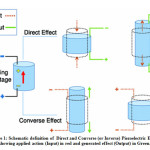

![Figure 5: Adopted from A Jbaily and RW Yeung (2015). There are many domains inside each grain or SXL.[19]](http://www.materialsciencejournal.org/wp-content/uploads/2020/08/Vol_17_2_Mat_Uda_Fig5.png)
![Figure 6: Adopted from reference.[19] Explanation of poling process, vide text.](http://www.materialsciencejournal.org/wp-content/uploads/2020/09/Vol_17_2_Mat_Uda_Fig6-150x150.jpg)
![Figure 15: Variation[5] of reflection effectiveness, 10 log (Prefl/Pin), with frequency, of 6 composites our Polymeric Binder (PB) with one or more of CdO-800, BaTiO3 (BT), Brass turnings (Brass) and Copper turnings (Cu) in compositions, listed in the Figure with Sample Name and Symbol. This is in the frequency range 26 GHz to 40 GHz.](http://www.materialsciencejournal.org/wp-content/uploads/2020/09/Vol_17_2_Mat_Uda_Fig15-150x150.jpg)
![Figure 19: TOF-ERDA raw data on our 1175°C fired Mg-O, scatterplot of recoil energy vs. time of flight – different traces for different elements. Large intensity (red) of Mg and O compared to impurities or surface contaminations can be noted. It is not ideal for presently used pellet sample that can have trapped moisture etc. [13]](http://www.materialsciencejournal.org/wp-content/uploads/2020/09/Vol_17_2_Mat_Uda_Fig19-150x150.jpg)
![Figure 20: Cd:O for “CdO” from ERDA after 36 h firing at different temperatures.[13]](http://www.materialsciencejournal.org/wp-content/uploads/2020/09/Vol_17_2_Mat_Uda_Fig20-150x150.jpg)
![Figure 21: Thermogravimetry of as-supplied cadmium oxide in air for heating at the rate of 1 ºC /min.[13,46]](http://www.materialsciencejournal.org/wp-content/uploads/2020/09/Vol_17_2_Mat_Uda_Fig21-150x150.jpg)
![Figure 22: Differential Scanning Calorimetry (DSC) of as-supplied cadmium oxide in air for heating rate of 1 ºC /min.[13,46]](http://www.materialsciencejournal.org/wp-content/uploads/2020/09/Vol_17_2_Mat_Uda_Fig22-150x150.jpg)
![Figure 23: 1.4 GeV Pb-ion irradiation[57] on SmFeAsO1−xFx crystal, with layered structure](http://www.materialsciencejournal.org/wp-content/uploads/2020/09/Vol_17_2_Mat_Uda_Fig23-150x150.jpg)