The Binary Oxide NiO-CuO Nanocomposite Based Thick Film Sensor for the Acute Detection of Hydrogen Sulphide Gas Vapours
Umesh Jagannath Tupe1 , M. S. Zambare1, Arun Vitthal Patil2 and Prashant Bhimrao Koli3*
1Department of Electronic Science, Fergusson College, Pune,(Maharashtra), India
2Department of Physics, Arts, Science and Commerce, College, Surgana, Taluka- Surgana,District- Nashik, (MH), India,
3Department of Chemistry, Arts, Commerce and Science College, Nandgaon, Taluka-Nandgaon, District- Nashik, (MH), India,
Corresponding Author E Mail: prashantkoli005@gmail.com
DOI : http://dx.doi.org/10.13005/msri/170308
Article Publishing History
Article Received on : 5-October-2020
Article Accepted on : 30-Nov-2020
Article Published : 10 Dec 2020
Plagiarism Check: Yes
Reviewed by: Dr.Suresh Ghotekar
Second Review by: Dr. Amlana Panda
Final Approval by: Jit satyabrata
Article Metrics
ABSTRACT:
The present research deals with the synthesis of copper oxide and nickel oxide nanoparticles. The nano powder of both NiO-CuO was utilized to fabricate the thick films.Thick films fabricated by screen printing method on glass substrate. The ex-situ doping method was followed for mixing the concentration of nickel oxide in copper oxide lattice. Calculated stoichiometric amount of NiO was loaded during thick film synthesis of CuO.The structure morphology of prepared CuO-NiO nanocomposite thick films was confirmed from x-ray diffraction technique, whichapproves cubic and crystalline CuO-NiO binary nanocomposite. The surface characteristics of the prepared films investigated byscanning electron microscopy that shows homogeneous, porous CuO-NiO nanoparticles with varying dimensions.The prepared thick films of CuO-NiO nanoparticles were analysed for electrical parameter, that assured the prepared material has a semiconducting nature. Further, these thick films promoted for gas sensing interpretation of H2S gas at various temperature and varied gas concentration. Here exclusive reports for hydrogen sulphide gas are reported. The binary CuO-NiO was thoroughly investigated for hydrogen sulphide gas concentration from 50 ppm to 500 ppm at the different temperature. The binary oxide sensor is found to be very sensitive at room temperature and maximum sensitivity response was 75.01 % for H2S gas. Furthermore the response and recovery times are also reported for binary sensor in the present research. The sensor reproducibility cycle was performed forbinary oxide sensor at hydrogen sulphide gas (H2S).
KEYWORDS:
H2S; NiO-CuO thick film sensor: SEM; Sensor reproducibility; TEM; XRD
Copy the following to cite this article:
Tupe U. J, Zambare S. M, Patil A. V, Koli P. B. The binary oxide NiO-CuO nanocomposite based thick film sensor for the acute detection of Hydrogen Sulphide gas vapours Mat. Sci. Res. India; 17(3).
|
Copy the following to cite this URL:
Tupe U. J, Zambare S. M, Patil A. V, Koli P. B. The binary oxide NiO-CuO nanocomposite based thick film sensor for the acute detection of Hydrogen Sulphide gas vapours Mat. Sci. Res. India; 17(3). Available from: https://bit.ly/37NTRQl
|
Introduction
The material science is now become a central hub for all research activities. Since there is very vast use of material science in countless fields of engineering technology and science. The use of various nanomaterials is highly desirable in the innumerable sections of science like electronics, sensors, transducers, photovoltaics, solar cells, biosensors etc. The extra ordinary results of materials in various fields is making great contribution in the field of research. The researcher’s community is strengthening all the possible sides of material science in overall application to serve the mankind better [1-5]. The important use of material science is to fabricate the classic and advanced nanomaterial for their intended use in various disciplines. These tiny nanoparticles have great inherent and potential properties such as excellent surface area, high thermal stability, extra ordinary catalytic properties, good mechanical, electrical and magnetic properties. Thus, these remarkable properties of nanoparticles encouraging the scientist community to get more incredible work with the ease of nanotechnology [7-9]
Today, the whole cosmos is facing the severe problem of pollution. Particularly, air and water pollution are big threat for the mankind. Most of the researchers are working on pollution related problem, to get rid of from the pollution and similar problems. The research community has focussed their views on utilization of nanobased catalyst to used in various forms in field of science and technology [10-14]. The large number of chemical industries releasing huge range of chemical gases in various forms with excess quantity that are quite poisonous in nature and spoiling the plants and animal life in many ways. From present reported medical data, it can be easily concluded that various harmful diseases like lung cancer, chronic obstructive pulmonary (COP) disease, stroke, acute respiratory infection, asthma etc, are reported solely due toxic chemical gases released by the industrial exhausts. Thus, this serious problem must be treated to get rid of from the potential hazardous diseases, since environmental safety has become prime importance in the recent time. [15-20].
The various toxic gases emerged from various industrial outlets can be detect in the modern technology by means of gas sensors. There are various chmirestive gas sensors have been reported by researcher community, which are quite effective to sense large number of pollutant gases typically emerged out from industrial exhausts. The common gases such as NOX, CO2, CO, CH4, SO2, SO3, H2S etc release to the atmosphere in large amounts. The typical metal oxide-based sensor in the form of thick and thin films are being utilized by the researchers to sense these toxic and harmful gases. Since method of preparation and cost is highly economical to prepare the metal oxide-based gas sensors and the ability of sensing the various according to the reports is also very high. Initially the gas sensors of single material like ZnO, SnO2, NiO, CdS, etc. were utilized to sense the various gases. Now binary oxides, nanocomposites and highly sensitive material are composed to prepare the thick and thin film gas sensors [21-22].
In the present research we have composed binary oxide bases thick film sensor fabricated using conventional screen-printing method. The binary oxide consists of combination of NiO into CuO nanomaterial. The thick of binary oxide NiO-CuO was utilized to sense the H2S gas vapours. Since according to reports H2S gas is also one of the poisonous gas after its threshold toxicity limit. According to reports hydrogen sulphide gas can have some common toxic effects on human being like coughing, chest pain, stomach pain, vomiting, headache, fatigue, loss of appetite, dizziness, poor memory, respiratory tract irritation etc. Hence, in this research we focus on the sensing of hydrogen sulphide gas by means of binary NiO-CuO based thick film senor. Here, we got almost 75% sensitivity for H2S for prepared NiO-CuO thick film senor. Additionally, we have reported selectivity, response -recovery and reusability for prepared thick film sensor.
Material and Methods
All the in synthetics utilized in amalgamation are of AR grade bought from Modern Laboratories Nashik, and utilized without any additional refinement. Chemicals required for the synthesis of copper oxide-nickel oxide binary nanocomposite are ammonia, sodium hydroxide, doubledistilled water, BCA, ethyl cellulose etc.
Synthesis of copper oxide by sol-gel method
Nanocrystalline copper oxide prepared by a common sol-gel course utilizing copper acetic acid derivation Cu (CH3COO). H2O as a source of copper metal.In the synthesis method of copper oxide nanoparticles, the calculated weight of copper acetate 1.82 g(0.01M), blended along with 20 ml of CH3-OH and agitated continuously at 60°C for 1-hour,the dark colour sol was converted to gel after continue heating for 30 minutes. The cyan coloured copper oxide was synthesized. The prepared copper oxide powder was calcined at 650°C in silica crucible under muffle furnace for 3 hours, the nanocrystalline copper oxide nanoparticles were collected from silica crucible for further use.
Synthesis of nickeloxide byco-precipitation method
Nickel oxide nanoparticles fabricated by cost effective sol-gel course, with the aid of ethanol and strong base sodium hydroxide. For synthesis, nickel chloride was dropped into 70 ml ethyl alcohol with incredible mixing at approximate 80 0C. At that point modest quantity (0.5 gm) of sodium hydroxide was solvated under ethyl alcohol in a different beaker. The basic solution of sodium hydroxide base at that point added to the nickel chloride solution drop by drop with steady mixing for 120 minutes. The light green color sol was formed here, with consistent warmth treatment, this sol was changed into gel. At first this gel was dried under IR light for 25 minutes. This, gel was squashed into fine powder by utilization of mortar and pestle. After this, the fine nickel oxide nanoparticles were calcined in silica pot for four hours at 700 0C. The blacked hued nickel oxide nanoparticles were recuperated from silica pot.
Preparation of NiO-CuO binary oxide thick film sensor by conventional screen-printingmethod
The binary oxide nanocomposite based thick film sensor was constructed by standard screen-printing technique. The binary oxide to binder ratio was maintain as 70: 30 respectively. The metal oxide (NiO-CuO) is considered to be inorganic part, while the binder material used was butyl carbitol acetate (BCA) and ethyl cellulose (EC). These both organic materials utilized as binders have a fixes ration of 8% to 92 % respectively, which are utilized to make films firm over the glass substrates. All these stoichiometric amounts of metal oxide and binders then mixed into mortar and pestle and crushed continuously for nearly 30 minutes. Then, BCA was mixed into above crushed powder of metal oxide and binders. This BCA was added drop wise to get gel like paste which can employed over glass film substrate. The prepared and well mixed paste was then applied on previously cutted glass films with 1.5X 2 cm dimensions.After complete coating of the films, these films were air dried firstly for 20 minutes followed by IR drying for 30 minutes. Finally, the prepared binary oxide film sensor was kept in muffle furnace for calcination process at 400 0 C nearly 120 minutes.On the next day the binary thick film oxide was recovered from muffle furnace to utilized for further study.
Thickness measurement of the films
The coated surface (thickness) of the films calculated by the use weight altered method as given in equation (1). After calculations the binary oxide NiO-CuO has thickness observed as 3330 nm. As per these calculations and thickness value, the prepared thick film sensor observed in the thick region.
t = ΔW / A ρ ———————————- equation (1)
ΔW = Weight difference of the film sensor after and before coating, ρ = combined density, A= area of the film (length*breadth)
Results and discussion
X-ray Diffraction (XRD)
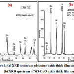
The NiO: CuO binary thick film sensor characterized by x-ray diffraction method. The XRD spectra of prepared thick film sensor is as shown in figure 1, clearly indicating the formation of crystalline NiO: CuO nanocomposite material. The Braggs diffraction peaks can be assigned to the formation of undoped copper oxide as depicted in Fig.1-a. The diffraction peak at the reflection planes (110), (002), (111), (202), (020), (202), (11), (220) can be attributed to the formation of undoped copper oxide material, which was confirmed from match scan data 80-1917.While the NiO loaded copper oxide XRD data as shown in Fig.1-b.Here the reflection planes can be assigned to formation of NiO doped copper oxide material. The NiO peaks observed with the planes (200), (220), (311) while, characteristics CuO planes observed at (113), (311), (133). This all diffraction data obtained confirms the formation of undoped CuO and NiO-CuO binary oxide material, which was confirmed from match scan data 78-0643. The cubic crystal structure is observed for NiO loaded CuO thick film. The mean nanoparticle size was determined by utilizing Debye-Scherer’s formula (equation 2).
[D = Kλ/β COS θ] —————————- equation (2)
where D is mean particle size, K is consistent (0.9 to 1), β is full width half maxima (FWHM) of diffracted top, θ is the point of diffraction. For simple CuO (without NiO), the mean particle size was 23 nm, while for binary oxide NiO-CuO, the mean particle size determine was 40 nm. The XRD spectrum of both these oxides thick films sensor is as depicted in Figure 1a-b.
Figure 1: (a) XRD spectrum of copper oxide thick film sensor (b) XRD spectrum ofNiO-CuO oxide thick film sensor
Scanning Electron Microscopy
SEM is often used to examine the surface characteristics of materials. SEM analysis of the materials can visualize various surface properties in the form homogeneous, heterogeneous, porosity, voids present over the surface. The undoped copper oxide and NiO-CuO thick films sensors were examined by SEM before gas detecting tests over the films. The surface and porosity of copper oxide nanoparticles as appeared in Figure 2 a-b. From SEM results it can be seen that the material possess various sized nanoparticles, has heterogeneous surface, and small void or cavities can be observed. The organize pictures of undoped CuO and NiO-CuO thick films shows the different measured nanoparticles with small interstitial spaces that be very efficient for gas occlusion and improved sensitivity. Furthermore, the particular surface zone of undoped CuO and NiO-CuO determined utilizing the BET technique for circular shape particles from the equation 3. The surface zone, particles size determined from SEM is as appeared in Table.1 [7]
Sa = 6/ d * ρ ————————–equation (3)
Sa = film surface area, 6 (six) = constant, ρ is the combined density of the prepared film sensors, d= mean particle size prepared films sensors.
Table 1: Surface area and mean particle dimensions pre-mediated from SEM data
|
Fabricated sensor
|
Calcination
Heating
(0 C)
|
Calculated Size,
d (nm)
|
Calculated size
d nm (SEM)
|
Surface Area of films sensor
(m2/ g)
|
|
CuO sensor
|
350
|
23
|
145
|
2.224
|
|
NiO-CuO sensor
|
350
|
40
|
190
|
3.068
|
Figure 2: (a-b) SEM images of copper oxide. (c-d) SEM images of NiO-CuOthick film sensor.
Transmission Electron Microscopy
The crystal lattice of NiO-CuO binary thick film oxide sensor was investigated for transmission electron microscopy study. The TEM images of prepared NiO-CuO binary thick film oxide sensor can be seen from images given below in figure 3 a-d. From the figure it can be seen that various oval,shaped crystals of prepared NiO-CuO lattices. The prepared crystals of NiO-CuO materials from 50-100 nm scale with various agglomeration can be easily seen from the TEM images. The TEM images of prepared thick film sensor are in good in agreement with previous reported data.
Figure 3: (a-d) TEM images NiO: CuO thick film sensor
Electrical Characterization
The undoped and NiO doped copper oxide film sensor prepared by screen printing method were examined for electrical portrayal and gas distinguishing appraisals. The gas distinguishing execution was evaluated by home-made gas sensor gathering. Reliably, the DC resistance of film sensor was surveyed by utilizing half increase approach, in the atmosphere of various temperature. The temperature sense by thermo couple was intentionally recorded by temperature recorder. The gas obsession in ppm level is presented inside the glass chamber perceiving gadget at the base of mechanical party by strategies for delta pipe. The length of the line valve finishes close to the film sensor with the target that the contact between film sensor and gas should be commonly ludicrous. The fixed DC voltage was applied to the circuit. The opposition of the movies was surveyed by utilizing yield voltage advanced multimeter. At every illustration of gas presented inside the glass chamber, gas advancement was pulled back by lifting the glass chamber and fixed temperature was given to free the gas improvement from the film. The oxygenated air was permitted to encounter the chamber at every ga affectability cycle. The results got from electrical depiction are addressed in Figure 4 a-b.
The gas distinguishing properties of undoped CuO and 3% Ni changed CuO was analysed at different raised temperature from 3500C to room temperature. The electrical obstacle of the thick film sensor was assessed inside seeing air without presentation of some different gases in the glass-domed chamber with the standard course of action as depicted in Figure 4-a. The average semiconducting nature of undoped CuO and NiO loaded CuO is as showed up in Figure 4 a-c. Figure 4 b-d shows the plot of log R against 1/T structure which the establishment essentialness has been investigated for declined and raise temperature district. The film resistance of the undoped CuO and NiO-CuO film sensors was dictated from following condition (4)
ρ = R.b.t / L —————— equation (4)
ρ = Resistance of prepared film sensors, R = resistance at normal temperature, b = breadth of film, t = thickness of the sensor film, L = length of the sensor film
The activation energy of CuO and NiO-CuO film sensor was commutated using following equation (5).
R = R0 e -ΔE/KT —————– equation (5)
R = Resistance at elevated temperature, R0 = Resistance at 00C, ΔE/T = activation energy, ΔE = 2.303 × K ×Slope, K= Boltzmann constant
Figure 4: (a) Plot of resistance against temperature undoped CuO (b) Plot of Log R verses 1/T for ΔE/T undoped CuO (c) Plot of resistance against temperature NiO: CuO sensor (d Plot of Log R verses 1/T for ΔE/T of NiO: CuO
Table 2: Calculations for ΔE/T and Resistivity forCuO andNiO: CuO sensor
|
Thick film sensor
|
D
(nm)
|
TCR
/oC
|
Resistivity
(Ω m)
|
ΔE/T
(eV)
|
|
Low temperature
|
High
temperature
|
|
CuO sensor
|
23 nm
|
-0.01257
|
112.4 x 10 3
|
0.1564
|
0.3717
|
|
NiO-CuO sensor
|
40 nm
|
-0.02351
|
149.9 x 10 3
|
0.20139
|
0.2299
|
Sensitivity and Selectivityof CuO and NiO-CuOfor Hydrogen Sulphide(H2S) gas
The optimum gas sensitivity of undoped CuO and 3% NiO doped CuO is as reported in Figure 5 a-b. Where the maximum response is reported in case of undoped CuO is 69.91 % for hydrogen sulphide gas vapours at room temperature. While the enhanced sensitivity is observed in case of 3% NiO doped CuO. The maximum response observed for doped copper oxide thick film sensor is 75 % at room temperature for hydrogen sulphide gas vapours. The increment in gas response for 3% NiO loaded CuO thick film is can be attributed more available surface area, declined band gap and enhanced conductivity of prepared sensor. The response enhancement is also due to addition dopant concentration of NiO in the CuO lattice
Figure 5: (a) The optimum selectivity of undoped CuO for H2S gas at 100 ppm. (b) The optimum selectivity NiO: CuO for H2S gas at 100 ppm.
Response and PPM Variation for CuO and NiO-CuO film sensor
The elevated gas response for undoped CuO and NiO stacked CuO against the ppm variation is as appeared in Figure 6 a-b. In this case rate reaction and gas accumulation in ppm was read for hydrogen gas sulphide fumes. Both sensors materials the reaction of the gases was observed to be improve with lift in gas fixation presumably because of aggregation of more gas atoms on the outside of sensors. The regular chemisorption of responding vaporous particles on sensor surface answerable for increasing the reaction of gases. The variety in gas reaction with PPM variety is as spoken to Figure 6 a-b.
Figure 6: (a) Recorded responses for H2S gas against ppm variation for undoped CuO. (b) Recorded response for H2S gas againstppm variation forNiO -CuO film sensor
Reusability ofNiO-CuO for hydrogen sulphide gas
The reuseability experiment for 3% NiO-doped CuO thick film sensor was performed in 4 cycles with a time interval of 15 days. The main object of reusability was to investigate the results reproducibility of sensor for hydrogen sulphide gas. The optimum response given by 3% NiO-doped CuO for H2S was 75 %, whether the same results are reproduced by the thick film sensor was investigated in the experiment. With a time interval of 15 days in four turns, a slight decrease in response was observed for H2S due to sight deterioration inhomogeneity of prepared thick film sensor of 3% NiO-doped CuO. The results obtained in the experiment are expressed in Figure 7
Figure 7: Reusability for NiO:CuO sensor for hydrogen sulphide gas Conclusions
In the present research, nanocrystalline CuO and NiO have been synthesized by a sol-gel and co- precipitation methods respectively. CuO-NiO thick films were constructed by screen-printing technique by using glass substrate. Structural characterization of samples showed that the undoped CuO thick films had a polycrystalline monoclinic crystal structure, while NiO material found to with cubic crystal structure. The sensitivity of H2S gas found to be highest to CuO-NiO thick film than pure thick film of CuO due to enhanced surface area and doping concentration of NiO. The dopant concentration of NiO found to be effective in reducing the distance between valence band and conduction band. The declined band gap also found to be effective to enhance the electrical and conducting, surface properties of the prepared NiO-CuO thick film sensor. The reuseability experiment for 3 % NiO loaded copper oxide thick film sensor showed that the prepared sensor is highly selective for hydrogen sulphide gas and the prepared sensor is selective, sensitive, and stable for frequent utilization of the prepared NiO loaded copper oxide thick film sensor.
Acknowledgments
Authors are gratefully acknowledged to the Department of Physics, Savitribai Phule Pune University, Pune providing facilities for XRD,SEM analysis. Authors are thankful to SAIF IIT Bombay for TEM analysis. Authors are very thankful to Department of Electronic Science, L. V. H. College, Panchavati, Nasikand Department of Electronic Science, Fergusson College, Pune for providing necessary laboratory facilities. Authors are also thankful to arts, commerce and science college, Nandgaon for providing necessary laboratory facilities.
Funding Source
This research received no specific grant from any funding agency.
Conflict of Interest
The authors have no conflicts of interest to disclose.
References
- S.J. Patil, A.V. Patil, V.G. Dighavkar, K.S. Thakare, R.Y. Borase, S.J. Nandre, N.G. Deshpande, R.R. Ahire, Semiconductor metal oxide compounds-based gas sensors: a literature review, Front. Mater. Sci. 9 (2015) 14–37.
CrossRef
- X. Liu, S. Cheng, H. Liu, S. Hu, D. Zhang, H. Ning, A survey on gas sensing technology, Sensor 12 (2012) 9635–9665.
CrossRef
- Y.F. Sun, S.B. Liu, F.L. Meng, J.Y. Liu, L.T. Kong, J.H. Liu, Metal oxides nanostructures and their gas sensing properties: a review, Sensors 12 (2012) 2610–2631.
CrossRef
- Koli, P.B., Kapadnis, K.H. and Deshpande, U.G. Study of physico-chemical properties, detection and toxicity study of organic compounds from effluent of MIDC Thane and GIDC Ankleshwar industrial zone. Applied Water Science, 8(7) (2018) 196.
CrossRef
- C. Wang, L. Yin, L. Zhang, D. Xiang, R. Gao, Metal oxide gas sensors: sensitivity and influencing factors, Sensors 10 (2010) 2088–2106.
CrossRef
- D.E. Williams, Semiconducting oxides as gas-sensitive resistors, Sens. Actuators B 57 (1999) 1–16.
CrossRef
- Koli, P.B., Kapadnis, K.H., Deshpande, U.G., More B.P and Tupe, U.J. Sol-Gel Fabricated Transition Metal Cr3+, Co2+doped Lanthanum Ferric Oxide (LFO-LaFeO3) Thin Film Sensors for the Detection of Toxic, Flammable Gases: A Comparative Study. Material Science Research India, 17(1), (2020) 70-83.
CrossRef
- Koli, P.B., Kapadnis, K.H., Deshpande, U.G. and Patil, M.R. Fabrication and characterization of pure and modified Co3O4 nanocatalyst and their application for photocatalytic degradation of eosine blue dye: a comparative study. Journal of Nanostructure in Chemistry, 8(4), (2018) 453-463.
CrossRef
- Koli, P.B., Kapadnis, K.H. and Deshpande, U.G.Nanocrystalline-modified nickel ferrite films: an effective sensor for industrial and environmental gas pollutant detection. Journal of Nanostructure in Chemistry, 9(2) (2019) 95-110.
CrossRef
- N. Kaura, E. Cominia, N. Polia, D. Zappaa, G. S berveglieria, Nickel oxide nanowires growth by VLS technique for gas sensing application, Procedia Eng. 120 (2015) 760–763.
CrossRef
- Y. Li, J. Liang, Z. Tao, J. Chen, CuO particles and plates: synthesis and gas-sensor application, Mater. Res. Bull. 43 (2008) 2380–2385.
CrossRef
- E. Llobet, P. Ivanov, X. Vilanova, J. Brezmes, J. Hubalek, K. Malysz, I. Gracia, C.Cane,C.Correig, Screen-printed nanoparticles tin oxide films for high-yield sensor Microsystems, Sens. Actuators B 96 (2003) 94–104.
CrossRef
- D.M. Smyth, The effects of dopants on the properties of metal oxides, Solid State 129 (2000) 5–12.
CrossRef
- N. Yamazoe, New approaches for improving semiconductor gas sensors, Sens. Actuators B 5 (1991) 7–19.
CrossRef
- Shinde, V.S., Kapadnis, K.H., Sawant, C.P., Koli, P.B. and Patil, R.P. Screen Print Fabricated In3+ Decorated Perovskite Lanthanum Chromium Oxide (LaCrO3) Thick Film Sensors for Selective Detection of Volatile Petrol Vapors. Journal of Inorganic and Organometallic Polymers and Materials, (2020), 1-15.
CrossRef
- Koli, P.B., Kapadnis, K.H. and Deshpande, U.G. Transition metal decorated Ferrosoferric oxide (Fe3O4): An expeditious catalyst for photodegradation of Carbol Fuchsin in environmental remediation. Journal of Environmental Chemical Engineering, 7(5), (2019) 103373.
CrossRef
- Koli, P.B., Kapadnis, K.H. and Deshpande, U.G. Methanol gas sensing properties of perovskite LaFeO3 nanoparticles doped by transition metals Cr3+ and Co2+. J. Chem. Pharm. Res, 9(1), (2017) 253-259.
- Adole, V.A., Pawar, T.B. and Jagdale, B.S. Aqua‐mediated rapid and benign synthesis of 1, 2, 6, 7‐tetrahydro‐8H‐indeno [5, 4‐b] furan‐8‐one‐appended novel 2‐arylidene indanones of pharmacological interest at ambient temperature. Journal of the Chinese Chemical Society, 67(2), (2020) 306-315.
CrossRef
- Adole, V.A., Waghchaure, R.H., Pathade, S.S., Patil, M.R., Pawar, T.B. and Jagdale, B.S. Solvent-free grindstone synthesis of four new (E)-7-(arylidene)-indanones and their structural, spectroscopic and quantum chemical study: a comprehensive theoretical and experimental exploration. Molecular Simulation, 46(14), (2020) 1045-1054.
CrossRef
- Diwan, Mehdi H., Wasfi M. Kadem, and Ziad T. Khodair, AIP Conference Proceedings. Vol. 2144. No. 1. AIP Publishing LLC, 2019.
- Y. Wang, F. Qu, J. Liu, Y. Wang, J. Zhou, S. Ruan, Enhanced H2S sensing characteristics of CuO-NiO core-shell microspheres sensors, Sensors and Actuators B: Chemical (2014), http://dx.doi.org/10.1016/j.snb.2014.12.010
CrossRef

This work is licensed under a Creative Commons Attribution 4.0 International License.