Stannous Oxide Thick Film Nanosensors Design by Screen Printing Technology: Structural, Electrical Parameters and H2S Gas Detection Study
Umesh Jagannath Tupe1* , Arun Vitthal Patil2, Madhukar Sarvottam Zambare1 and Prashant Bhimrao Koli3
1Department of Electronic Science, Fergusson College, Pune,(Maharashtra), Affiliated to Savitribai Phule Pune University, Pune, India.
2Department of Physics, Arts, Science and Commerce, College, Surgana, Taluka- Surgana, District- Nashik, (MH), India, Affiliated to Savitribai Phule Pune University, Pune, India
3Karmaveer Abasaheb Alias and N.M Sonawane Arts, Commerce and Science College, Satana, Taluka-Baglan, District- Nashik, (MH), India, Affiliated to Savitribai Phule Pune University, Pune, India.
Corresponding Author Email: umeshtupe14@gmail.com
DOI : http://dx.doi.org/10.13005/msri/180108
Article Publishing History
Article Received on : 20-Nov-2020
Article Accepted on : 22-Mar-2021
Article Published : 23 Mar 2021
Plagiarism Check: Yes
Reviewed by: Dr. Abhijit De
Second Review by: Dr. B. Dilip Kumar
Final Approval by: Dr. Nagaraja K K
Article Metrics
ABSTRACT:
The present research deals with the fabrication of stannous oxide nanoparticles by conventional and cost effective co precipitation method. The thick film sensors of SnO2 nanoparticles were prepared by standard screen-printing technique by photolithography. The prepared SnO2 material was characterized by several techniques to confirm the structural properties. Initially, the prepared nanoparticles of SnO2 were investigated by x-ray diffraction technique to confirm the synthesis of prepared material within nanoscale. From XRD data the average particle size of prepared thick films was found to be 21.87 nm calculated using Debye-Scherer formula. The material was further characterized by using scanning electron microscopy (SEM) to investigate the structural and surface characteristic of SnO2. SEM data clearly indicates the heterogeneous surface, and some voids present over the surface of SnO2 nanoparticles. The Fourier transfer infra red technique was employed to investigate the metal oxygen frequency of SnO2 material. The prepared sensor was exclusively utilized to sense the hydrogen sulfide gas vapors at various concentrations. The prepared sensor was found to be highly sensitive to H2S vapors nearly 63.8% sensitivity was recorded. The response and recovery study shows the response time of 9 seconds and recovery time of 19 seconds for hydrogen sulfide gas vapors. The SnO2 sensor was further utilized for recycling performance to get the firm results of sensitivity in four turns with period of 15 days.
KEYWORDS:
H2S sensor; Reusability; Stannous oxide thick film sensor; Screen printing technology
Copy the following to cite this article:
Tupe U. J, Patil A. V, Zambare M. S, Koli P. B. Stannous Oxide Thick Film Nanosensors Design by Screen Printing Technology: Structural, Electrical Parameters and H2S Gas Detection Study. Mat. Sci. Res. India;18(1).
|
Copy the following to cite this URL:
Tupe U. J, Patil A. V, Zambare M. S, Koli P. B. Stannous Oxide Thick Film Nanosensors Design by Screen Printing Technology: Structural, Electrical Parameters and H2S Gas Detection Study. Mat. Sci. Res. India;18(1). Available from: https://bit.ly/2OPVHLj
|
Introduction
Material science recently becomes more promising field in the catalysis and sensors technology. Most of the researchers are working on the material technology to defeat the environmental and industrial problems. Due to rapid urbanization and industrialization the pollution related problems are enhanced with high percentage leading to fatal toxic effects on human and animals. Thus, everyone is looking to get perfect remedy to get rid off from these pollution related problems. Material science has great potential to defeat these problems Since, most of the material prepared as sensors are easily employed to sense these toxic gases at various concentrations. The main air pollutants such as carbon dioxide, carbon monoxide, sulphur dioxide and NO2 etc. are responsible to make polluted environment 1-3. Hence, the similar gases must be detected with effective sensors. These gases are emerging as automobile exhaust and industrial by products and their desired concentration is highly toxic.
On the other hand there are several gases which are emerged during chemical reactions, as well as by products of several chemical processes and mining. The gases like hydrogen sulfide, VOC’s (volatile organic compounds), methane, and natural hydrocarbons etc. Out of these the hydrogen sulfide concentration at elevated level can be highly toxic and leads to fatality in many ways. According to research, nearly 700-800 ppm concentration of H2S leads to loss of consciousness, fatigue, breathing problem, cardiopulmonary arrest etc. Hence, the good sensors that can sense the hydrogen sulfide vapors will be very useful defeat H2S toxicity3, 4. Hydrogen sulfide (H2S) is colorless, more hazardous and toxic element. It can be identified by a characteristic rottenegg odor at small concentration. The major noticeable point of hydrogen sulfide is easily smelled perceptible at concentrations low concentration in air but if the concentration of gas is increases in the surrounding, smell is disabling. The presence of high concentration of hydrogen gas in the surrounding with no perceivable odor is extremely dangerous for human being, so it is necessary to control and monitor H2S gas in the environment 4, 5. The gas is inherently found in manure, hot springs, volcanoes, several sewage, swamps, geysers, by-products of several chemical reactions, mining etc.
There are several methods to prepare the nano particles some of the popular methods can be listed as physical vapor deposition (PVD), chemical bath deposition (CBD), spray pyrolysis, green synthesis method, sol-gel method, combustion method and co-precipitation method. Depending upon the requirement the method can be selected to synthesis the desired nanomaterials.The stannous oxide nano particles can be cost effectively synthesized by co-precipitation and sol-gel route.Many of the research papers flaunting that metal oxides nano particles can be useful as gas sensors for the most of the gases [6, 7].A great deal of efforts has been put into developing new sensing materials with improved sensor properties. The listed synthesis techniques can be easily employed to fabricate the various semiconducting nano sensors in low time and cost effective way 7, 8.
The tin dioxide (SnO2)is a versatile metal oxide because of its two characteristics; variable valence state and existence of oxygen vacancy defects. It has wide band gap of ~ 3.6 eV and it shows n- type semiconductor behavior. Tin dioxide also referred as tin oxide and stannousoxide. SnO2 has numerous special attentions in the field of material science due to their diverse applications like catalysis, transparent conducting oxides, battery materials, solar cell, optics and gas sensing etc.The stannous oxide sensors are effectively used to sense the various toxic gases as mentioned earlier as thin and thick film gas sensor 8, 9.
In the present research we are reporting the cost effective synthesis of SnO2 by co-precipitation method and its application for detection of H2S gas at various concentration and temperature.The structural and electrical properties of SnO2 thick films are also reported in the present investigations. In the present investigations the SnO2 thick film sensor was exclusively utilized to sense the hydrogen sulfide gas vapors. In addition to that the response and recovery curves and recycling properties are reported of SnO2 sensor for hydrogen sulfide gas vapors.
Material and Methods
The chemicals required for synthesis of SnO2 are sodium hydroxide, stannous chloride dihydrate, acetone, ammonia, and double distilled water. All the chemicals used were analytical grade and used without further purification. The screen printing apparatus was utilized to prepared stannous oxide thick film sensors.
Synthesis of SnO2 nanoparticles using precipitation method
SnO2 nanoparticles were synthesized by cost effective co-precipitation method. In this method, stannous chloride dihydrate used as source of tin (Sn). To prepare SnO2 nano particles initially, 0.01 moles of tin chloride dihydrate (SnCl2. 2H2O) were dissolved in 100 ml of double distilled water. In a separate beaker 0.1 molar solution of ammonia was prepared. Then, 0.1 a molar ammonia solution was dropped into tin chloride solution drop wise with constant stirring. The stirring was continued till white precipitate of tin hydroxide was obtained. The, white precipitate was filtered off, dried and calcined under muffle furnace at 400 ℃ for three hours. The white colour tin dioxide nano particles were recovered from muffle furnace on next day and used for further process of research.
Thick films preparation of SnO2 nano particles by using standard screen printing technique.
The thick films of pure SnO2 were prepared by using screen printing technique on glass substrate. The organic compounds used as binders and tin oxide nano particles were used in appropriate ratios as 30:70 respectively.The compounds used as binders over the glass substrates were 8% BCA (Butyl Carbitol Acetate) and 92% ethyl cellulose (EC). Where, inorganic composition used as tin oxide nano particles. Together, these both organic and inorganic compounds were mixed in mortar and pestle and mixed mechanically, the desired concentration of EC and BCA were added to get thixotropic paste.The prepared paste mass was then applied on glass substrate (previously cutted with 2.5×1.25 cm) by screen printing technology.Screen printing setup consists of nylon screen of 120 meshes to put paste on glass substrate. After complete coating of the films, the films were dried under IR lamp for 30 minutes. In these process IR radiations removes temporary organic volatile materials. Finally, films were annealed at 350ºCin the muffle furnace for 3 hours.The calcined films were used in further gas sensing and electrical study.
Thickness measurement of the films
The surface coating of the films was calculated using equation 1 as mentioned below. The thickness of the stannous oxide film sensor was calculated as 4.22 μm, (4220 nm). The thickness is observed in the thick region. The thickness of the SnO2 film sensor was calculated using mass difference method10, 11.
t = ΔM / A ×ρ ———————–equation (1)
ΔM = Mass difference of the film before and after deposition.
ρ = Composite density of stannous oxide film sensor SnO2
A= Area of the film
Results and discussion
X-ray diffraction study
The screen printed thick films of stannous oxide were investigated by means of x-ray diffraction technique model number D8 Bruker AXS (Germany), possessing Braggs scanning angle varying from 20-900. The instrument consisting CuKα (wavelength 1.51 A0) used to generate x-rays 12, 13. The XRD spectrum of stannous oxide thick films is as depicted in figure 1.The XRD spectrum as depicted in figure 1, from which the Bragg’s reflection peaks can be assigned to the formation ofSnO2 material having tetragonal crystal lattice with space groupP42/mnm 14, 15. The 2θ values of diffraction peaks gained from x-ray diffraction statistics for stannous oxide material are 26.18, 33.53, 38.26, 51.59, 54.10, 57.12, 61.14,65.18, 71.40, and 79.07. The two theta values as mentioned above can be assigned to reflection of ( 110), (101), (200), (211), (220), (002), (310), (112), (202), (321) planes. The diffraction peaks mentioned above with respective hkl planes confirms the formation tetragonal SnO2 crystal lattice. The average particle size was calculated from Debye- Scherer’s formula represented in equation 2
D = Kλ/β COS θ —————————– equation (2)
Where D is average particle size, K is constant (0.9 to 1), β is full width half maxima (FWHM) of diffracted peak, θ is the angle of diffraction. The average particle size of stannous oxide nano particles calculated using equation 2 was found to be 51.10 nm. The match scan data of stannous oxide exhibits the fabrication of SnO2 material with JCPDS cart number 00-001-0625.
Figure 1: XRD spectrum of SnO2 thick film
Scanning electron microscopy (SEM)
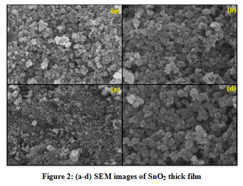
Figure 2 shows SEM image of pure SnO2 thick film. The 2D image with high magnification was used to study surface morphology of this film.SEM results indicate the formation of particles with different shapes and sizes. The image shows, larger particles or grain agglomeration16, 17. From SEM images it can be seen that the nano particles with varied size and diameter having voids and cavities over the surface of SnO2 nano particles. These voids are responsible for the adsorption of the gas molecules like H2S. The specific surface area calculated by using SEM images [18]. The diameter (d) of SnO2 nano particles was measured by using Image J software for spherical particles. The rate of adsorption and desorption increases with large surface area of the films and chemisorptions properties between adsorbent SnO2 nano particles and adsorbate gas molecules.Using BET method, specific surface area of SnO2 thick films was calculated by equation 3.Specific surface area of SnO2 material found to be 1.4312m2/g.
Sw = 6/ρ x d ————————–equation (3)
Where, d is the diameter of the particles and ρ is the density of the particles and Sw is specific surface area.
Figure 2: (a-d) SEM images of SnO2 thick film.
Energy-dispersive X-ray spectroscopy (EDAX)
Energy dispersive x-ray spectroscopy of SnO2 thick film samples fired at 350˚C was performed. From EDAX spectrum of SnO2 the elements tin and oxygen are well resoluted. From EDAX spectrum it can be seen that there is no other impurity elements were found in SnO2 thick films. From the EDAX scale of SnO2 it can be observed that the elemental tin is well resolute at 3.4 -4 KeV, while the elemental oxygen is resolute at 0.6-08 KeV 19-21. The EDAX results obtained for stannous oxide thick are in good agreement with reported results. Excess amount of oxygen observed in the E-DAX analysis, may be due to the adsorption of the oxygen during the sintering or firing stage of the SnO2 thick films21. Due to high electron affinity of surface molecules, oxygen gets attached to the molecules on the surface of the thick films.
Figure 3: EDAX spectrum of pure SnO2 thick film
Electrical Characterization
The electrical characterization of prepared SnO2 thick films studied in this section. The electrical characterization of sample performed by determination of resistivity (ρ), the activation energy (∆E ) and the temperature coefficient of resistance (TCR)21.
Figure 4: Resistance measurement and gas sensing apparatus
Resistivity of SnO2 thick film
Resistance determination of SnO2 thick films was done using home built characterization system shown in figure 4. Resistance of SnO2 thick films was determined by using half bridge method. In half bridge method the value of Rref =10 MΩ and 30VDC power supply were used. The resistanceof the thick film samples was determined using following equation 420, 21.
Rsample = Rref [ (Vsupply /Vref ) -1]———- equation (4)
The resistivity of prepared thick films was measure as function of temperature with range 30- 350 oC by using half bride method. Readings of temperature verses voltage were taken with the interval of 10oC temperature. The resistance of SnO2 thick films found to be decreasewith increase in temperature. This confirms thetypical semiconductingbehavior of SnO2 material by obeying R= R0e-∆E/KT in the 30 oC- 350 oC temperature range21. Figure 5shows the change in resistance of pure CuO thick films with respective change in temperature.
Figure 5: Resistance verses temperature for SnO2 thick film.
Figure 5 indicates that the resistance of SnO2 thick film decreases rapidly from room temperature (30 oC) to certain temperature range and at the higher temperature range the resistance decreases slowly. The exponential nature of graph shows the resistance reaches steady lowest saturation level with respective temperature 22-24. The resistivity of SnO2 thick films at constant temperature is calculated using the equation 5.The resistivity of SnO2 thick film is found to be 2.76 Ω-m.
ρ = R.b.t / L —————— equation (5)
ρ = Resistivity of the film,
R = resistance at room temperature,
b = breadth of film,
t = thickness of the film,
l = length of the film.
To calculate resistivity of thick film, R = 24×10 8Ω, L= 2.5 cm, b= 1.25 cm and t= 23µm were used.
Activation Energy of stannous oxide thick film material
The activation energies of prepared SnO2 thick films was measured at the low temperature and high temperature, the activation energy of SnO2 film was calculated using Arrhenius plot.Figure 6 shows graph of log Rin ohm versus reciprocal of temperature (1/T) in oK for SnO2 thick films. The Arrhenius plot indicates two distinct regions of temperature low and high temperature region respectively. The annealing temperature of films plays a very important role to decide the transition temperature from low region to high region. The Activation energy for SnO2 thick film found 0.2767 eV and 0.5988 eV at low and at high temperature respectively. The energy of activation within the low temperature region is often but the energy within the high temperature region because material passes from one conduction mechanism to a different. In the low temperature region ,the increase in conductivity is because of the mobility of charge carrier, which is rely upon the dislocation concentration. The conduction mechanism is typically called the region of temperature conduction, during this region energy of activation decreases because atiny low thermal energies quite sufficient for the activation of charge carriers to require part within the conduction process. Hence increase in conductivity within the lower temperature region may be attributed to the rise of charge mobility.
Figure 6: Arrhenius plot for SnO2 thick film
Temperature Coefficient of Resistance (TCR) of SnO2 thick film material
The temperature coefficient of resistance (TCR) of pure SnO2 thick films is calculated by using below equation 6.Temperature coefficient of resistance is found negative to pure SnO2 thick film samples. The negative sign indicate the semiconductor behavior of the prepared pure SnO2 thick films. High resistivity of thick film samples corresponds to a low TCR value. TCR of pure SnO2 thick film is found 1.006×10⁻³ K-1.

Table 1: Electrical outcome for SnO2 thick film
|
Resistivity
(Ω m)
|
Activation Energy
(eV)
|
TCR
/ K-1
|
|
Low temperature
|
High
temperature
|
|
2.76
|
0.2767
|
0.5988
|
1.006×10⁻³
|
Study of H2S gas sensing characterization of SnO2 thick film.
The major objective of the current research work was to focus on the study of hydrogen sulfide (H2S) gas sensing mechanism and the optimum selectivity of H2S gas toward the prepared stannous oxide thick films. Resistance of the film was measured in the form of voltage using half bridge method. This method is applied at different operating temperatures in H2S gas atmosphere for pure SnO2 thick films. The H2S gas was injected with different concentration level in ppm at normal atmospheric conditions.The basic principle of metal oxide semiconductor (MOS) is when gas molecules interact with the surface of semiconducting films its resistance varies.By using this gas sensing principle the current study of gas sensitivity was carried out. Operating temperature is an important parameter for gas sensing mechanism [25]. Therefore, the determination of operating temperature of SnO2 thick film to test H2S gas was the main objective. On the basis of measured data sensitivity, repeatability and reproducibility of thick film gas sensing results were interpreted.
Gas sensitivity properties of SnO2 at elevated H2S gas concentration.
The H2S gas sensing behavior of pure SnO2 thick films was studied by using home-built static apparatus. Pure SnO2 thick film resistance was measured by using half bride method with temperature in the H2S gas atmosphere. Time interval of operating temperature is 50oC during the measurement of gas response. For measurement of H2S gas sensitivity the temperature range varied from room temperature 35oC to 250 ºC. The gas sensitivity of the prepared SnO2 thick film was calculated using equation 7.
% Sensitivity = Ra-Rg / Ra × 100 —————– equation (7)
Where, Ra– Resistance in air and Rg–Resistance H2S gas atmosphere.
The concentration of H2S gas in the current gas sensing study were taken in parts per million (ppm). Here four concentrations viz.100 ppm, 200 ppm, 500 ppm and 1000 ppm of H2S gas were used for gas sensing purpose. From Figure 7, SnO2 thick film showed 63.8 % sensitivity to H2S gas at operating temperature at 200ºC and gas concentration 500 ppm.H2S gas also shows good response to 200 ppm at 200 oC. The response of H2S gas slowly increases to 100 ppm concentration with increase in temperature. It has been observed that when nano particles of SnO2 were exposed to the H2S gas, the resistance of thick film decreases because the nature of H2S gas is reducing. At 500 ppm concentration of H2S gas SnO2 thick film show more sensitivity as compare to 100 and 200 ppm. It has been also found that at 1000 ppm of gas concentration sensitivity decreases.
Figure 7: Sensitivity of H2S gas for SnO2 thick film sensor.
Response time and recovery time
The thick film sensor was kept at 200oC optimum temperature. Then, H2S gas was injected using syringe in the glass dome of the gas sensing system for measurement of response time. To determine response time variation in resistance is measured with time 25. From figure 8 it was observed that response time is 08 seconds whereas recovery time was 20 seconds to SnO2 thick film sensor for H2S gas at concentration 500 ppm and at 200 oC optimum temperature.
Figure 8: Response and recovery time of SnO2 thick film for H2S gas.
H2S gas sensing mechanism toSnO2 thick film sensor
The SnO2 thick film sensor shows good response to H2S gas. SnO2 is n-type semiconductor and the majority of charge carriers in n type semiconductors are electrons. H2S is reducing gas, when a molecule of hydrogen sulfide gas comes in contact with the surface of SnO2 thick film sensor the sample resistance decreases due to adsorption reaction and sensor gives response to H2S gas25.
Reusability of SnO2 thick film sensor for hydrogen sulphide gas
The SnO2 thick film sensor reusability experiment was carried out in four cycles with a 15days interval between each cycle. The main goal of the reusability study was to see whether the results of a hydrogen sulphide gas sensor could be repeated. The optimum response for H2S provided by SnO2 was 63.8 %, and the experiment looked into whether the thick film sensor could replicate the same results. In the second turn the optimum response for H2S gas was 62.48%, in the third the response found to be 61.13% and in the final set, the optimum response was recorded as 60.65%. It may be due to sight variation in composition of the prepared thick film sensor of SnO2, minimum decline in response for H2S was observed after 15 daysinterval in four turns. Figure 9 depicts the reusability outcomes of the experiment.
Figure 9: Reusability for SnO2 thick film sensor for hydrogen sulphide gas.
Conclusions
From the obtained results, nano crystalline powder of SnO2 has been fabricated by using co-precipitation method. SnO2 thick films were prepared by standard screen printing technique on glass substrate. From XRD data it is observed that synthesized SnO2 nano particles belongs to tetragonal lattice. The SnO2 thick film sensor showed nearly 63.8 % sensitivity at 200 oC temperature. The structural and electrical investigation supports SnO2 is good semiconducting material with optimum activation energy. The reusability experiment performed for SnO2 thick film sensor proved that the sensor is promising for hydrogen sulfide gas vapors for long time stability and reusability.
Acknowledgment
Authors are very thankful to Department of Electronic Science, L. V. H. College, Panchavati, Nasik and Department of Electronic Science, Fergusson College, Pune for providing necessary laboratory facilities.Authors are gratefully acknowledged to the Department of Physics, Savitribai Phule Pune University, Pune providing facilities for XRD,SEM analysis.
Conflict of Interest
There are no Conflict of interest.
Funding Source
This research received no specific grant from any funding agency.
References
- Baumbach, Günter. Air Quality Control: Formation and Sources, Dispersion, Characteristics and Impact of Air Pollutants—Measuring Methods, Techniques for Reduction of Emissions and Regulations for Air Quality Control. Springer Science & Business Media, 2012.
- X. Liu, S. Cheng, H. Liu, S. Hu, D. Zhang, H. Ning, A survey on gas sensing technology, Sensor 12 9635–9665, 2012.
CrossRef
- Patil, Sunil Jagannath, et al. “Semiconductor metal oxide compounds based gas sensors: A literature review.” Frontiers of Materials Science 9.1, 14-37, 2013.
CrossRef
- Tabassum, Rana, Satyendra K. Mishra, and Banshi D. Gupta. “Surface plasmon resonance-based fiber optic hydrogen sulphide gas sensor utilizing Cu–ZnO thin films.” Physical chemistry Chemical physics 15.28,11868-11874(2013).
CrossRef
- Tupe, U.J., Zambare, M.S., Patil, A.V. and Koli, P.B., The Binary Oxide NiO-CuO Nanocomposite Based Thick Film Sensor for the Acute Detection of Hydrogen Sulphide Gas Vapours. Material Science Research India, 17(3), (2020) 260-269.
CrossRef
- Wang, Yuliang, and Younan Xia. “Bottom-up and top-down approaches to the synthesis of monodispersed spherical colloids of low melting-point metals.” Nano letters 4.10 , 2047-2050,2004.
CrossRef
- Biswas, Abhijit, et al. “Advances in top–down and bottom–up surface nanofabrication: Techniques, applications & future prospects.” Advances in colloid and interface science 170.1-2 ,2-27, 2012.
CrossRef
- Srivastava, Abhilasha, et al. “Study of structural and microstructural properties of SnO2 powder for LPG and CNG gas sensors.” Materials chemistry and physics 97.1 ,85-90, 2006.
CrossRef
- Jain, Kiran, R. P. Pant, and S. T. Lakshmikumar. “Effect of Ni doping on thick film SnO2 gas sensor.” Sensors and actuators B: chemical 113.2, 823-829, 2006.
CrossRef
- Koli, P.B., Kapadnis, K.H., Deshpande, U.G., More B.P and Tupe, U.J. Sol-Gel Fabricated Transition Metal Cr3+, Co2+doped Lanthanum Ferric Oxide (LFO-LaFeO3) Thin Film Sensors for the Detection of Toxic, Flammable Gases: A Comparative Study. Material Science Research India, 17(1), (2020) 70-83.
CrossRef
- Koli, P.B., Kapadnis, K.H., Deshpande, U.G. and Patil, M.R. Fabrication and characterization of pure and modified Co3O4 nanocatalyst and their application for photocatalytic degradation of eosine blue dye: a comparative study. Journal of Nanostructure in Chemistry, 8(4), (2018) 453-463.
CrossRef
- Garje, A. D., and S. N. Sadakale. “LPG sensing properties of platinum doped nanocrystalline SnO2 based thick films with effect of dipping time and sintering temperature.” Advanced Materials Letters 4.1, 58-63, 2013.
CrossRef
- Ibarguen, C. Ararat, et al. “Synthesis of SnO2 nanoparticles through the controlled precipitation route.” Materials Chemistry and Physics 101.2-3, 433-440, 2007.
CrossRef
- Gaber, A., et al. “Influence of calcination temperature on the structure and porosity of nanocrystalline SnO2 synthesized by a conventional precipitation method.” Int J Electrochem Sci 9.1, 81-95, 2014.
- Naje, Asama N., Azhar S. Norry, and Abdulla M. Suhail. “Preparation and characterization of SnO2 nano particles. ” International Journal of Innovative Research in Science, Engineering and Technology 2 ,7068-7072, 2013.
- Martinelli, Giuliano, and Maria Cristina Carotta. “Thick-film gas sensors.” Sensors and Actuators B: Chemical 23.2-3 ,157-161 1995.
CrossRef
- Zargar, Rayees A., et al. “Synthesis and characterization of screen printed ZnO films for solar cell applications.” Optik 126.23 , 4171-4174, 2015.
CrossRef
- Patil, A. V., et al. ” Formulation and Characterization of Cr2O3 Doped ZnO Thick Films as H2S Gas Sensor.” Sensors & Transducers 108.9 ,189, 2009.
- Koli, P.B., Kapadnis, K.H. and Deshpande, U.G.Nanocrystalline-modified nickel ferrite films: an effective sensor for industrial and environmental gas pollutant detection. Journal of Nanostructure in Chemistry, 9(2) (2019) 95-110.
CrossRef
- Koli, P.B., Kapadnis, K.H. and Deshpande, U.G. Transition metal decorated Ferrosoferric oxide (Fe3O4): An expeditious catalyst for photodegradation of Carbol Fuchsin in environmental remediation. Journal of Environmental Chemical Engineering, 7(5), (2019) 103373.
CrossRef
- Patil, A. V., et al. “Effect of firing temperature on electrical and structural characteristics of screen printed ZnO thick films.” Journal of Optoelectronic and Biomedical Materials 1.2 (2009): 226-233.
- J. Zheng, W. Xiaojuan, Z. Bing, G. Huijiao, L. Tiebing and W. Minghong, “Effects of Electron Beam Irradiation on Tin Dioxide Gas Sensors,” Bulletin of Materials Sci-ence, Vol. 31 No. 1, , pp. 83-86.(2008).
CrossRef
- Hyo-Jin Ahn, Hyun-Chul Choi, Kyung-Won Park, Seung-Bin Kim,Yung-Eun Sung, “Investigation of the Structural and Electrochemical Properties of Size-Controlled SnO2 Nanoparticles”, J. Phys. Chem. B, Vol.108, pp.9815-9820, (2004).
CrossRef
- Marikutsa, A. V., et al. “Nanocrystalline tin dioxide: Basics in relation with gas sensing phenomena. Part I. Physical and chemical properties and sensor signal formation.” Inorganic Materials 51.13 1329-1347, (2015)
CrossRef
- Balaguru, R. John Bosco, and B. G. Jeyaprakash. “Mimic of a gas sensor, metal oxide gas sensing mechanism, factors influencing the sensor performance and role of nanomaterials based gas sensors.” NPTEL–Electrical & Electronics Engineering–Semiconductor Nanodevices ,2004.
- Khanna, Atul, Rajesh Kumar, and S. S. Bhatti. “CuO-doped SnO2 thin films as hydrogen sulfide gas sensor.” Applied physics letters 82.24, 4388-4390, 2003.
CrossRef

This work is licensed under a Creative Commons Attribution 4.0 International License.