K. Arun Vasantha Geethan1 and S. Jose2
1Department of Mechanical Engineering, Sathyabama University, Chennai, India.
2Alpha College of Engineering, Chennai, India.
DOI : http://dx.doi.org/10.13005/msri/070122
Article Publishing History
Article Received on : 15 Mar 2010
Article Accepted on : 25 Apr 2010
Article Published :
Plagiarism Check: No
Article Metrics
ABSTRACT:
Reliability prediction is fundamental to system design. It involves the quantitative assessment of systems reliability prior to development. For many years the reliability of an electronic system was based, to a great extent, upon the junction temperatures of the semiconductor devices. Substantial efforts were made in the fabrication methods, mounting methods, and cooling techniques of the electronic devices to reduce these hot spot temperatures below 100 °C. This has produced a significant improvement in the reliability and effective operating life of the equipment. However, the electronic failure rates are still too high. Additional reductions in the failure rates must be achieved to further improve the reliability of our electronic equipment. Some of the failure mechanisms that can cause malfunctions in electronic systems are examined in this paper Experience has shown that most of these failures are produced by a mismatch in the thermal coefficients of expansion (TCE) of the different types of materials typically used in electronic assemblies. The mismatch often generates high forces and stresses, which produce fractures and cracks in the electronic components and assemblies. An examination of a large number of avionics failures has shown that most of them are mechanical in nature. They typically involve fractures in solder joints, electrical lead wires, plated through holes (PTH), electrical cables, connectors, adhesive bonded joints, and hermetic seals. These failures are often produced by various combinations of thermal, vibration, shock, humidity, and salt environments, combined with poor manufacturing processes and poor design practices. These failures must be reduced in order to achieve a substantial improvement in the system reliability. The paper aims at presenting the numerical evaluation by finite element analysis of the common class of PCBs under the mechanical stress. This work contributes to the study of vulnerability in packaged electronics by comparing the numerical result with finite element analysis.
KEYWORDS:
Reliability; Thermal coefficient of expansion; PCB; Malfunctions; Mechanical stresses; Finite element analysis.
Copy the following to cite this article:
Geethan K. A. V, Jose S. Evaluation of Stresses in Flame Resistant Materials. Mat.Sci.Res.India;7(1)
|
Introduction
Electronic assemblies utilize a wide variety of plastics and metals in the fabrication and manufacturing of their products. These materials can have significant differences in their thermal TCE, which may result in high strains and stresses in the lead wires, solder joints, and PTH if these factors are not understood or if they are ignored. Temperature changes will produce dimensional changes in almost all materials normally used in the assembly of electronic chassis and PCBs. Dimensional changes can occur due to power cycling where the power is turned on and off, which induces temperature changes within the electronic assembly. This can also be caused by thermal cycling, where the outside ambient temperature changes and the thermal lag within the chassis forces thermal gradients to develop because of different mass effects. These dimensional changes, which can occur along the X, Y, or Z axes of the electronic assemblies, can produce a wide variety of failures in the structural elements of these assemblies.
Problem Statement
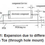
A large number of components such as resistors, capacitors, diodes, flat packs, and hybrids are fabricated with axial leads. Wire-forming tools are then used to bend the leads 90° for insertion in through hole PCBs for flow soldering. During exposure to thermal cycling environments, the PCB typically ‘ has a higher TCE than the component in the X-Y plane, so the PCB will expand more than the component. Since the wire in an axially leaded component has a relatively low bending stiffness, virtually all of the deflection difference between the PCB and the component will be taken up by the bending in the wire, as shown in Figure below. A bending moment will be developed in the wire, at the PCB solder joint, which will produce a bending stress in the lead wire. This stress value should be limited to achieve a better operating life.
Figure 1: Expansion due to difference in Tce (through hole mount)
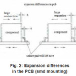
The PCB contains glass fibers which have a low TCE. This reduces the TCE of the PCB in the X and Y planes, so the PCB expands and shrinks less than the transformer. This expansion difference produces the high forces in the lead wires. The wires transfer the load to the solder pads, lifting the pads, which are only cemented to the surface of the PCB.
Figure 2: Expansion differences in the PCB (smd mounting)
Scheme 1
Results and Discussion
In order to analyse the reliability of the PCB we selected an emergency LED lamp which is a consumer product.This product is launched in the market as three different variants each one having a different PCB compositions.The different compositions are
FR-2
FR-3
FR-4
To determine the stresses developed in the components we have considered a pcb mounted with a component i.e a CF resistor body(through hole mount),copper core transformer(surface mount)
Evaluating the Exsisting Parameters
The thermal expansion of the PCB will be greater than the expansion of the resistor because the TCE of the PCB is greater than the TCE of the resistor. The expansion differences will force the vertical leg of the resistor lead wire to bend. This action will produce bending and shear stresses in the lead wires, and shear tear-out stresses in the solder joints.
Deflection (Xw)
XW= ap Lp Δt –ar Lr Δt-ah Lh Δt (inches) (eqn1)
ap= TCE of PCB in X-Y plane, LP = effective length of PCB, Δt = total temperature range,
Δt = neutral to peak value for a rapid temperature cycle,
aR = TCE of carbon composition resistor,
LR = half of resistor body length, aH = TCE of horizontal copper wire ,
LH = horizontal length of lead wire
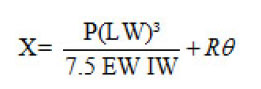
Load (P)
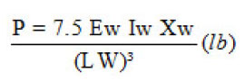
LW= effective wire length,
EW =copper wire modulus elasticity,
IW=moment of inertia of wire
Bending moment (M)
M=1.2PLw Lb in
Bending stress
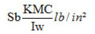
(Iw=πr4/64)
Bending stress
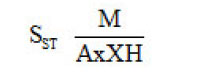
As= area of shear
H= height of board
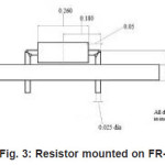
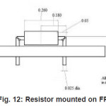
For FR-2
Composition: phenolic resin
Figure 3: Resistor mounted on FR-2
XW=3.074e-05 in
P= 0.165 lb
M=0.01485 lb in
Sb= 9683.09 psi
SST=265.9 psi
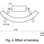
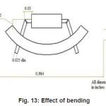
Effect of Bending in PCB
When the PCB bends, the magnitude of the horizontal load will be reduced. When bending in the vertical member of the lead wire and rotation of the PCB is considered, this cause a rotation of the vertical lead wire. The horizontal displacement expected at the top of the wire will be the sum of the wire bending and the PCB rotation, as shown in, when the horizontal and vertical legs of the wire are the same length. Now the combined deflection equation becomes
Where
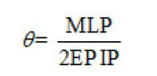
Therefore
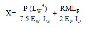
Figure 4: Effect of bending
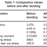
M =bending moment on PCB, EP=PCB modulus of elasticity, LP = length of PCB between component lead wires, Ip=moment of inertia of PCB. For the same value of deflection the load and bending stress becomes
P=0.160 lb
Sb=9389 psi
Therefore the percentage reduction in load and bending stress will be 3.03%.
Table 1: Comparative values before and after bending
Finite Element Analysis
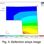
Deflection
Figure 5: Deflection ansys image
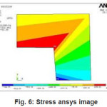
Stress (sb) before considering bending
Figure 6: Stress ansys image
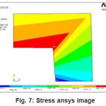
Stress (sb) after considering bending
Figure 7: Stress ansys image
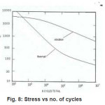
No. of cycles. Increased
Figure 8: Stress vs no. of cycles
No. of cycles increased for FR-2 Material is 250 cycles
For FR-3
FR3 is also basically FR2.But instead of phenolic resin it uses an epoxy resin binder
Table 2: Comparative values before and after bending
Finite element analysis
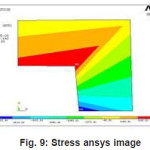
Stress (sb) before considering bending
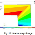
Figure 9: Stress ansys image
Stress (sb) after considering bending
Figure 10: Stress ansys image
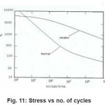
No. of cycles. Increased
Figure 11: Stress vs no. of cycles
No. of cycles increased for FR-2 Material is 150 cycles.
For FR-4
FR4 is a glass fiber epoxy laminate. It is the most commonly used PCB material (0.06inch). FR4 uses 8 layers glass fiber material
Figure 12: Resistor mounted on FR-4
Figure 13: Effect of bending
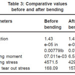
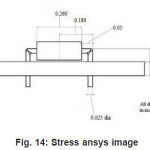
Table 3: Comparative values before and after bending
Finite element analysis
Stress (sb) before considering bending
Figure 14: Stress ansys image
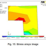
Stress (sb) after considering bending
Figure 15: Stress ansys image
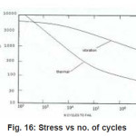
No. of cycles. Increased
Figure 16: Stress vs no. of cycles
No. of cycles increased for FR-4 material is 350 cycles
Result for Problem Statement 1
From the figures ,8,11 and 16 we can clearly see that FR-4 give us the maximum increase in the no. of cycles when the stress is reduced. This depicts that FR-4 is the most reliable base material for manufacturing a PCB
Sol 2
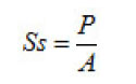
Thermal expansion differences between the transformer and the PCB in the X-Y plane will produce a force on the lead wires and cause them to bend. This same force will produce a shear stress in the solder joint at the junction of the lead wire and the PCB. The direct shear stress (Ss) in the solder joint can be obtained from the solder pad area. This direct shear stress does not include solder joint stresses produced by the overturning moment. Both stresses may be combined to obtain the maximum or the Von Mises stress. Only the shear stresses were used here to determine the approximate fatigue life of the solder joint. Stress concentrations are not considered here because the solder is so plastic.
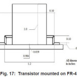
Figure 17: Transistor mounted on FR-4
Here deflection is X=(aT – aP) b Dt=2.613e-04 in
Iw = 1.917e-08(cylindrical lead wire)
( Iw=πd4/64)
Using
eqn 2 : P=0.601 lb
eqn 3: M=0.072 lb in
eqn 4: Sb= 47034 lb/in2 (Beyond safe value)
This far exceeds the ultimate tensile stress of 45,000 psi for the copper lead wire, which means that the wire will be in the plastic bending range. However, analysis with this condition shows that the probability of a wire failure is low if there are no sharp cuts in the wire.
Hence evaluating the direct shear stress we get
Where solder pad A =2.25e=03
(0.09×0.025)
Ss=267.11 lb/in2
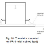
Reducing the Thermal Expansion Forces
Lower forces and stresses in the electrical lead wires and solder joints will lead to a longer life with a higher reliability. This shows that the forces in the lead wires can be reduced by decreasing the moment of inertia (Iw)
Decreasing the Moment of Inertia I
The moment of inertia of the component wire can be reduced by coining (squeezing or rolling) the round wire into a flat thin rectangular cross section. This will decrease the force in the wire, which will decrease the wire bending stress and the solder joint shear stress. Coining will also increase the width of the lead wire at the solder joint, which will increase the solder joint area and further reduce the solder joint stress.
IW = 6.66e-09 (rectangular cross section)
(IW =bd3/12)
Therefore
P =0.2088 lb (using eqn2)
= 29.03
Where the solder pad area is (0.09 X0.08)
Therefore the percentage reduction in shear stress will be 89
Figure 18: Transistor mounted on FR-4 (with coined lead)
Result for Problem Statement 2
Therefore by changing the cylindrical cross section of the lead wire to a rectangular cross section the value of direct shear stress is reduced by 89%
Conclusion
Thus from the above reliability analysis on electronic components we can conclude that the life of the electronic packages can be increased to a considerable no. of cycles by reducing the stress induced in it. The different types of component mounting techniques have different alternative solution for reducing the value of stress which was discussed formerly.
References
- Navy Power Supply Reliability—Design and Manufacturing Guidelines, NAVMAT P1955-2 (1988).
- Erdogan F.Stress distribution in a non homogenous elastic plane with cracks.J Appl Mech 30: 232-6 (1963).
CrossRef
- Erdogan F.Stress distribution in bonded dissimilar materialswith cracks.J Appl Mech., 32: 403-10 (1965).
CrossRef
- Analysis of Thermal Failure of Electronic Components Chiraq university
- Amagai M, Umeda Y.Mechanical characteristics of die attach materials in ball grid array packages. J IMAPS Microcircuit Electron Packag., 20(4, Fourth Quarter):482-93 (1997).
- Irwin GR.Analysis of stresses and strains near the end of a crack traversing a plate.J Appl Mech., 24: 361-4 (1957).
- Yu Q, Shiratori M.Thermal fatigue reliability assessmenfor solder joints of BGA assembly. ASME EEP, vol. 26–1.Adv Electron Packag. 1: 239-46 (1999).
- Omiya M, Kishimoto K, Shibuya T, Amagai M.Effect of intermetallic compound layer development on interfacial strength of solder joints. ASME EEP-vol. Adv Electron Packag 1: 11 (2001).
- Amagai M.Cracking failure in lead-on-chip packages. IEEE Trans CPMT Part B: Adv Packag. 18(1): 119-26 (1995).
- Introduction to Electronic Failure Analysis,digital engineering library.

This work is licensed under a Creative Commons Attribution 4.0 International License.