K. Vijaylakshmi and C. Ravidhas
Department of Physics, Bishop Heber College, Tiruchirappali, India.
DOI : http://dx.doi.org/10.13005/msri/070134
Article Publishing History
Article Received on : 30 Oct 2009
Article Accepted on : 02 Dec 2009
Article Published :
Plagiarism Check: No
Article Metrics
ABSTRACT:
ITO is the most commonly used semi conducting materials for sensor devices. In the present work. Transparent conducting ITO films have been deposited on to glass substrates by rf magnetron sputtering at 648k Temperature under an oxygen partial pressure of 10x10-3 mbar, The deposition condition necessary to produce ITO films with high conductivity and optical transparency over a wide spectral range were studied and optimized. The more influential factors determining the optical and electrical properties including partial pressure of the reactive gas The sputtering power as well as other growth related effects is analyzed. Transmission was measured with perkin–Elmer–UV/VIS lambda 40 spectrometer and electrical studies using four probe and Hall effect setup. Structural characterization of the films has been done by XRD. Characterization of the coatings revealed specific receptivity's below 6.5 10-3Ω. Films deposited without annealing were amorphous and the crystallinity improved after annealing at 700k. the optical transmittance of the SEM appears to be uniform over large surface areas. The correlations among properties of the film and its influence on heat treatment have been analyzed. The obtained results have been used for a better comprehension of the gas–sensing properties towards. NO2.
KEYWORDS:
ITO sputtering parameters; Annealing; NO2 Gas sensor
Copy the following to cite this article:
Lakshmi K. V, Ravidhas C. NO2 Sensing Properties of Nano Structured ITO Thin Film. Mat.Sci.Res.India;7(1)
|
Introduction
Development of gas sensing devices is in the focus of activity of scientists and engineers in many countries in the last two decades.1,2 Such detectors can be used for different applications like detection of toxic dangerous gases, drugs, smoke and fire. Energy saving as well as various technological processes in industry.3 Nitrogen dioxide is a hazardous gas which affects the environment and human health.4 Hence there is a great interest in developing chemo resistive gas sensor based on metal oxides for the detection of the low concentration of NO2 for air quality monitoring.
Suitable semiconductor materials currently needed, which have required surface an bulk properties and high sensitivity. Stability and selectivity.5 a wide variety of material including SnO2 and In2O3 have been tried for NO2 detection. but the sensing properties combined in a binary form are not completely known and demands further exploration. Owing to the excellent stability of ITO as compared to the problem of drift common with tin oxide materials. Use of ITO is very promising for NO2 detection. The resistively is in the range of 10-3 to 10-4 Ωcm making it easy to be interfaced with opto electronic circuits.6
Several deposition techniques have been repotted for the production of ITO films like chemical vapour deposition.7 Spray pyrolysis.8 Electron beam evaporation [9] etc. Among these rf sputtering seem to be quite promising. Because sputtering provides high uniformity of the thickness of the deposited film. Better reproducibility of the film. Good adhesion to the substrate, ability of the deposit to maintain the stoichiometry of the original target composition.10
Experimental
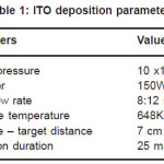
Indium tin oxide thin film were deposited on glass substrate using RF magnetron sputtering. The ITO target is prepared using In2O3 having 15% SnO2 (Alfa Aesar product.) The distance between target and substrate was approximately 7 cm. All the substrates were ultrasonically cleaned in isopropyl alcohol (propan– 2–ol) and dried. The deposition process was carried out under an oxygen partial pressure of 10×10-3 mbar. The RF power was varied from 100-200 W and kept constant at 150 W during all the processes. The deposition were done at 648K temperature for 25 minutes and annealed at 700K for lH. The optimized deposition parameters for the preparation of ITO thin films in the present study are summarized in Table l. Finally optical, electrical and structural properties of the ITO films were studied. Transmission was measured with Perkin–Elmer-UV/VIS lambda 40 spectrometer Sheet resistance was measured with 4 point probe and surface profile meter was used for thickness measurement. The crystallographic orientation of the ITO films was determined by an X–ray diffractometer (XRD) using Cu Kα irradiation. The morphology of ITO films was investigated by Scanning Electron Microscopy (SEM).
Table 1: ITO deposition parameters
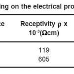
Table 2: Effect annealing on the electrical properties of the ITO film
The films so optimized with deposition conditions were used to fabricate the gas sensor in the desired geometry with two thick gold pads on two sides of the film to take out electrical contacts. An airtight chamber made of Borosil glass with gas inlet and outlet valves wherein the sensor mounted on a heater is housed. The gas injection is to be carried out using calibrated digital micro– pipette. In order to inject the gas easily. The chamber is evacuated to a base pressure of 10-2 Torr using an oil free vacuum pump. The substrate is kept at a chosen temperature using a pt–heater and the values of temperature are measured by the Ni–Cr thermocouple. Two gold electrodes are placed on the surface.
Of the film which made ohmic contact with the film. The temperature is controlled by varying the current flow through the heater and measured with an accuracy of ±1oC using a temperature controller cum indicator. Electrical resistance measurement is made in the temperature range from 350K to 700K in air ambient. This resistance is considered as a reference value for the calculation of sensitivity. After noting this, the test gas is injected inside the chamber and all the valves are closed to avoid the leakage of the gas. The resistance of the sensor in once again measured for different temperature in gas–air ambient. The sensitivity for oxidizing gases is defined using the relation S = Rg/Ra- Where Rg and Ra the resistance of the sensor in the testing gas and in the air respectively.
Results and Discussion
Effect of r.f. Power on Sheet Resistance of the Film
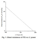
The r.f. power has a direct influence on the deposition rate and the induced voltage as well as generating heat due to the electron bombardment intrinsic to this technique11. After experimenting with various. r.f. power for ITO deposition a marked influence is seen on the electrical properties of the deposited film. The results from depositions using an oxygen partial pressure of 10×10-3m bar show that the sheet resistance Rsh of the ITO films are inversely proportional to the expontial of the r.f. power used as shown in fig. 1. Films grown at 100W showed typical Rsh of about 45KΩ/Sq. at 150W this was 12KΩ/sq while at 200w the Rsh was 35KΩ/sq. it should be noted that these values were obtained without any post–deposition annealing: however films deposited at 200W were reported to be difficult to etch [12.13]: hence the r.f. power of 150 W was used for all subsequent work. Also, from sensing application point of view, the use of excessive r.f. power is not suitable.
Figure 1: Sheet resistance of ITO vs r.f. power
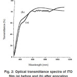
Figure 2: Optical transmittance spectra of ITO film (a) before and (b) after anncaling
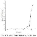
Figure 3: Graph of (hυα)² vs energy for ITO film
Effect of Annealing on Structure and Morphology of the Film
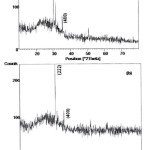
Structural characterization of the films has been done by XRD. The X-ray diffraction pattern of ITO films is obtained by XPERT – PRO unit. The film surfaces are found to be smooth and adherent to the substrate. Fig. 4 (a) and (b) shows the diffraction pattern of the films before and after annealing respectively. All diffraction peaks are indexed with JCPDS card file (006-0416) [16] and corresponding peaks are identified. The cell parameter was calculated as 10.24A. The diffraction patterns show the presence of (222) phase in the films. Studies on ITO films have shown that the different energy state of sputtered particle brings about different texture formation [17]. Extremely high energetic sputtered particles prefer the (4 0 0) orientation in the big diffraction angle 2ègreater than 34o region . while relatively energetic particles prefer the (2 2 2 ) orientation in the small diffraction angle 31 – 32o region. However the (2 2 2) orientation has been reported as the preferred orientation for ITO film sputtered from metal alloy or oxide targets by many works. It was observed that there is an overall increase in the peak heights upon annealing the film.
Figure 4: XRD pattern of the ITO film (a) before annealing (b) after annealing
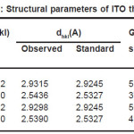
The mean grain size was determined using Schrerrer’s formula [118] by measuring FWHM of (222) peak and it was found to be 56nm. The observed interplanar spacing between the planes of the crystal lattice were compared with the standard data and the calculated values of grain size. Dislocation density and number of crystallites is presented in table 3. As the temperature was increased the sharpness and intensity of (400) diffraction peak also increased which indicated a preferred orientation along (100) direction. This is because of the improved crystalline upon post–deposition annealing probably because of the incorporation of sn-2 in the In+3 sites in the presence of the oxygen. Thus annealing provided restructuring of the film leading it to be better polycrystalline nature.
Table 3: Structural parameters of ITO thin film
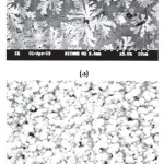
Scanning Electron Microscopy was used to study the morphology and thickness of the film. Fig. 5 shows the SEM photographs of ITO films before and after annealing respectively. The SEM analysis before annealing shows a nano scaled system with a non uniform morphology with a bright and flower shaped agglomerates of nano grains. After annealing the film shows a fine, uniform and closely packed distribution of polycrystalline nano clusters without micro cracks. The effect of annealing improves the structural homogeneity and the degree of crystallinity of the film. The average grain size calculated in proportion to the photos is about values are well corresponded to these determined by XRD.
Figure 5: SEM photographes of the ITO film (a) before annealing (b) after annealing
Sensing Properties of ITO
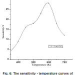
After having optimized the deposition parameter for ITO films. The device was fabricated as a resistive type gas sensor. NO2 is a highly reactive species showing an oxidizing character with respect to non stoichiometric metal oxide [19]. Hence, promoting the deviation from stoichiometry and decreasing the resistance of the coated ITO thin film can be a strategy for improving the performance of the materials as NO2 sensor [20]. The sensor working temperature that regulates the adsorption/desorption processes at equilibrium and the competition for chemisorptions between NO2 and atmospheric oxygen O2 for the same active surface sites play an important role in determining the specific interaction between the gas and sensor. Fig. 6 shows the variation in sensitivity of the ITO sensor with operating temperature in the presence of NO2 gas. The gas concentration was kept constant at 50ppm. It is observed that the surface redox state of the element changes with temperature with the highest sensitivity at 600k. due to mixing of two different oxide phases which imparts higher dispersivity and defectiveness of the materials.
Figure 6: The sensitivity-temperature curves of ITO sensor
NO2molecules are highly reactive species showing a oxidizing character with respect to nonstoichiometric metal oxide. and may decompose into other materials on adsorption sites. If there are no stable adsorption sites for NO2 on the ITO thin film sensor, some NO2 molecules will decompose and desorb from the sensor, which inhibits the net adsorption of NO2 At. Low temperature, a direct ionosorption at the active film surface takes place as
NO2.gas +e → NO- 2,ads
At higher temperature. With a considerable surface coverage of O- 2.ads ions. NO2 react with O- 2.ads ions forming nitrato complexes NO- 3.ads .
NO2.gas +O-2,ads → NO- 3.ads
Therefore higher working temperature will accelerate decomposing and desorbing of NO2-and we get a higher sensitivity at low concentration. By suitably adjusting working temperature. The ITO gas sensor can adapt applications in both low and high NO2 concentration.
Conclusion
Nano crystalline Type semi conducting ITO thin films were deposited by rf sputtering on glass substrate. it was observed that film properties greatly depend on deposition condition and suggest that a careful optimization of growth parameters as well as post – deposition treatment is necessary for reproducible results. Sheet resistance Rs h decreased drastically after annealing at 700 K temperature. This significant reduction in the Rsh is due to the large increase in the mobility and further suggest that this may be associated with the increase in grain size of the film. Optical studies reveal that the average visible transmittance is above 80% regardless of annealing atmosphere and it is improved after annealing. The change in the resistivity ρ of the film with annealing is very similar to the corresponding change in the sheet resistance resistance XRD spectrum confirm the polycrystalline, nature of the film and the intensity of (400) diffraction peak also increased. This suggests that there is minimal structural change to the ITO films following annealing, most likely due to the increased carrier concentration. Which is known to cause an increase in the absorption edge of ITO. SEM micrographs of the film shows a uniform and closely packed distribution of polycrystalline nano clusters without micro cracks. The ITO film so optimized with the deposition condition show best response to NO2 gas, especially to concentration lower than 50 ppm. At 600K the sensor shows higher sensitivity to NO2. due to the presence of two different metal cation ions which imparts more heterogeneity to the active surface of the sensor.
Acknowledgements
This work was financially supported by University Grants Commission (MRP – 2575/08) which is gratefully acknowledge.
References
- A. Amaral, P. Brogueira, C. Nunes de Carvalho and G. Lavareda, Optical Materials 17: 291 (2001).
- N.G. patel. K.K. Makhija, C.J. panchal. D – B dave, V.S. vaishnav, Sensors and Actuators B 23: 49 (1995).
- R. Tueta. M. Braguier. Thin Solid films 80: 143-148 (1981).
- R. Teghil, V. marotta, A. Giardini Guidoni,T.M.Di palma. C.flamini. applied surface science 138: 522-226 (1999).
- B. Besais, N. mliki and R. Bennaceur, semiconductor science and technology 8:116-121 (1993).
- V. S. vaishnav, P.d. patel, N.g. patel, thin solid films 487: 277-282 (2005).
- A. tanusevski, Semicond. Sci. Technol 18:501-505 (2003).
- A.M.Ezhil Raj, K. Vijayalakshimi, G. Selvan,M. Jayachandran, C. Sanjeeviraja, journal of non–crystalline solids 354: 3773-3779 (2008).
- Hamid Reza Fallah, Mohsen Ghasemi, Ali hassanzadeh, Physical E: Low – dimensional systems and Nano structures 39: 69-74 (2007).
- C. Baban, Y. Toyada, M.Ogita, thin solid films 488: 369-373 (2005).
- C.V.R.V.kumar and A. mansigh, Journal of Applied Physics 65: 1270-1280 (1989).
- J.C.C.fan and F.J.Bachner, Journal of Electrochemical Society Solid State Science and Yechnology 122: 1719-1725 (1975).
- I. Adesida, D.G. Ballegeer, J.W. Seo, A. Katterson, H.Chang,K.V.cheng & T.Gessert, Journal of Vacuum Science and TechnologyB9: 3551-3554 (1991).
- H.W.Zhang and W.Xu,Vacuum 43: 835-836 (1992).
- C.H.L.Weijtens, Journal of Electrochemical Society 138: 3432-3434 (1991).
- Jin Ma, Shu – ying Li,Jun – Qing Zhao, hong– Lei Ma, thin solid films 307: 200 (1997).
- F.H. Mullins and A.Brun schweiller Solid State Electronics, 19: 47-50 (1976).
- B.D. Cullity, ‘Elements of X ray diffraction’ Addition – Wesley, Massachusetts (1956).
- P.Menini, F.Parret, sens, actuators B 105:111-114 (2004).
- G.Xu Y.W.Zhang X.sun.C.L.Xu,C.H.yan,J.Phy.Chem.B 109: 3269-78 (2005).

This work is licensed under a Creative Commons Attribution 4.0 International License.