Anuradha C. Pawar1, A. V. Kokate2, Pradnya S. Raut3, J. A. Borase2, B. G. Wagh4 and H. R. Kulkarni2
1Department of Physics, Brahma Valley Polytechnic, Anjaneri, Nashik - 422 213, India.
2Department of Physics, MET's Institute of Engineering, Adgaon, Nashik, India.
3Department of Chemistry, MET's Institute of Engineering, Adgaon, Nashik, India.
4Department of Physics, KAANMS Arts, Commerce, Science College, Satana, Nashik, India.
DOI : http://dx.doi.org/10.13005/msri/070141
Article Publishing History
Article Received on : 25 Jun 2009
Article Accepted on : 30 Jul 2009
Article Published :
Plagiarism Check: No
Article Metrics
ABSTRACT:
ZnIn2Se4 thin film were prepared by pulsed electro deposition technique over stainless steel substrates in galvanostatics mode from an aqueous acidic bath containing ZnSO4, In Cl3, and SeO2. The growth kinetics of the film was studied and the deposition parameters such as electrolyte bath concentration, deposition time, current density, and pH of electrolyte bath are optimized. The X-ray diffraction (XRD) analysis of the deposited film showed presence of polycrystalline nature. The surface morphology studied by Scanning electron microscope (SEM) shows that the deposited film are well adherent and grains are uniformly distributed over the surface of substrate.
KEYWORDS:
Electrodeposition; XRD; SEM; Kinetics; ZnIn2Se4
Copy the following to cite this article:
Pawar A. C, Kokate A. V, Raut P. S, Borase J. A, Wagh B. G, Kulkarni H. R. Studies on Growth Kinetics of Electrodeposited Znin2se4 Thin Films. Mat.Sci.Res.India;7(1)
|
Copy the following to cite this URL:
Pawar A. C, Kokate A. V, Raut P. S, Borase J. A, Wagh B. G, Kulkarni H. R. Studies on Growth Kinetics of Electrodeposited Znin2se4 Thin Films. Mat.Sci.Res.India;7(1). Available from: http://www.materialsciencejournal.org/?p=2336
|
Introduction
For the last couple of decade’s interest in the use of photo electrochemical solar cells lead to large amount of research in the search for thin film polycrystalline material with acceptable efficiency. Some time approaching that of single crystals. In recent years, thin films have attracted much interest because of their varied application such as semi conducting devices, photovoltaic, optoelectronic devices, radiation detectors, laser materials, thermoelectric devices, solar energy converters. etc.1-4
Interest in the use of photo electrochemical (PEC) solar cells for low-cost energy conversion has lead to an extensive research in the field for novel and suitable thin film semiconductor materials.5-8 Recent investigation has shown that layered type semi conducting zinc chalcogenide group (ZnSe, ZnS, ZnTe) which absorb visible and near IR light are particularly promising materials for photo electrochemical solar energy conversion. The polycrystalline electrodes are economically desirable for solar cell applications. Hence this study has been directed towards obtaining ZnIn2Se4 in polycrystalline thin films.
Many workers investigated the photo electrochemical property of ZnIn2Se4 single crystal. The structural and optical properties of electrodeposited ZnIn2Se4 thin films have been reported. Many workers have been succeeded in depositing thin film of ZnIn2Se4by vacuum evaporation.
In this report an attempt is made to prepare ZnIn2Se4 films through electrodeposition technique on stainless steel substrate which enables the film to be used for characterization studies like structural, surface composition, surface morphology and optical properties.
Material and Methods For Thin Film Synthesis
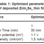
The thin films of ZnIn2Se4 were pulsed electro deposited on stainless steel substrate. The stainless steel plates were used as the cathode in three electrodes cell with graphite as the counter electrode and saturated calomel electrode (SCE) was the reference electrode. The electrolyte was prepared by mixing solution of ZnSO4 (0.1M), InCl3 (0.1M), and SeO2 (0.1M) in the ratio of 1:2:4 respectively. The pH of electrolyte solution was varied by dilute HCl. Double distilled water was used for preparation of aqueous solution of above precursor chemicals. Before deposition the substrate were thoroughly cleaned with double distilled water. The distance between the working electrode and counter electrode way kept constant as 1 cm during deposition. From visual observation it was observed that a formation of reddish films of ZnIn2Se4 take place. These pulsed plated ZnIn2Se4 films were found to be well adherent and uniform. The detailed growth kinetics was studies by changing the deposition parameters, the pH of solution and current density
Results and Discussion
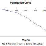
The polarization curve were plotted to determine the deposition potential of ZnIn2Se4 thin film are shown in fig 1.
Figure 1: Variation of current density with voltage
The concentration of Zinc sulphide (ZnSO4), Indium trichloride (InCl3), and selenium dioxide (SeO2) were 0.1M. The films were grown at the optimized deposition potential of 1100 mV with respect to SCE and at the current density 1.5 mA/ cm-2. When an electric field is applied between the working and counter electrode a fine ZnIn2Se4 thin film formation occurs on the surface of the substrate. The process of film formation is observed to be time dependent. The deposited film have been dried and preserved in desiccators for further study. The current density varied from 0.6 to 4.6 mA/cm–2 during deposition. The film deposited at current density 1.5 mA/cm-2 was found to be uniform thick. And well adherent to substrate. For other higher and lower values of current density thickness of film was less as compared to 1.5 mA/cm-2.
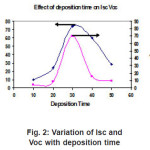
The PEC cell n-ZnIn2Se4 /polysulphide/c is illuminated with 200 w tungsten filament lamps. The photons having energy equal to or greater than band gap energy of ZnIn2Se4 are absorbed in semiconductor and the electron-holes pairs are generated these electron hole pair are separated by local electric field. Present across the interface between semiconductor and polysulphide electrolyte. This leads to generation of photo voltage under open circuit and photocurrent under short circuit condition. The variation of Isc and Voc as a function of deposition time at constant pH is presented in fig 2.
Figure 2: Variation of Isc and Voc with deposition time
It can be seen that the Isc and Voc are relatively higher at deposition time 30 min. at pH 2 this may be due to formation of nearly stoichiometric ZnIn2Se4 thin film material at 30 min.and optimum thickness of ZnIn2Se4 for the effective absorption of the photons. Fig 2 shows the variation of Isc and Voc with deposition time and the optimum values of Isc and Voc are found to be for the film deposited for 30 min. this may be attributed to the optimum thickness of the film.
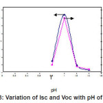
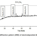
Fig 3 Shows that variation of Isc and Voc with different pH at constant deposition time. It can be seen that the Isc and Voc are relatively higher at pH =1 at deposition time 30 min and optimum pH of ZnIn2Se4 film for the effective absorption of photons. The grown ZnIn2Se4 film deposited at the optimized preparation parameter was further characterized by analyzing the X-ray diffraction (XRD) pattern. The XRD pattern of ZnIn2Se4 film deposited on stainless steel substrate is shown in fig.4.
Figure 3: Variation of Isc and Voc with pH of bath
Figure 4: The X-ray diffraction pattern (XRD) of electrodeposited ZnIn2Se4 thin film
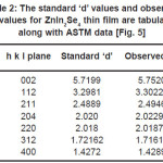
The XRD analysis reveals that film is polycrystalline and the sharp peaks are identified at (112), (211), (204) planes of ZnIn2Se4 film. The standard‘d’ values and observed ‘d’ values for ZnIn2Se4 thin film are matching with each other. (Table 2). This confirms that material is ZnIn2Se4
Table 1: Optimized parameters of deposited ZnIn2Se4 thin film
Table 2: The standard ‘d’ values and observed ‘d’ values for ZnIn2Se4 thin film are tabulated along with ASTM data [Fig. 5]
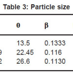
Table 3: Particle size
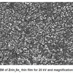
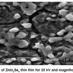
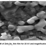
The surface morphology of ZnIn2Se4 thin film was studied by SEM picture.The SEM micrograph shows well adherent, smooth film surface without cracks. The surface morphology of ZnIn2Se4 film prepared under optimized conditions exhibits spherical grains of uniform size about 12A0 spread all over the surface.
Conclusions
Almost stoichiometric ZnIn2Se4 thin films formation by electro deposition technique was taken from acidic bath. The film grown at the optimized pH and time is polycrystalline with tetragonal structure and the particle sizes are found to be 10.705 A0 , 12.9429 A0 ,13.7332 A0 with lattice parameter a=5.709, b=5.709, c=11.44. SEM analysis is shown by Fig.5,6,7 indicating that the deposited film is uniform , well adherent and grains are uniformly distributed over the surface of substrate.
Figure 5: SEM of ZnIn2Se4 thin film for 20 kV and magnification is 1000
Figure 6(a): SEM of ZnIn2Se4 thin film for 20 kV and magnification is 5000
Figure 6(b): SEM of ZnIn2Se4 thin film for 20 kV and magnification is 10000
Acknowledgements
I would like to thank Prin. Prof. C.K.Patil, Prin. Dr.A.A.Kulkarni, all of my colleagues, staff members, and research scholars of the institute.
References
- K. Y. Rajpure, C. D. Lokhande and C. H. Bhosale. Mater. Chem. phy 252: 51 (1997).
- V.L.Mathe,K.Y. Rajpure and C.H.Bhosale Bull. Mater. Sci. 22: 927 (1999).
- N.G.Patel., Solid State Eelctrochem. 35: 1269 (1992).
- H.J.Goldsmid and J.E.Giutronich.M.M.Kalia., Solar energy 24: 435 (1980).
- X.Mathew and P.J.Sebastian, Solar Energy Mater., Solar Cells 59: 85 (1999).
- X.Mathew J. Phy D. Appl. Phy. 33: 1565 (2000).
- P.PHankare, S.D.Delekar, V.M.Bhuse, P.A.Chate, K.M.Goradkar. semiconductor Sci.Technol.20: 257 (2005).
- Y. Wade. Nishimatsl. J.Electrochem. sco. 125: 1499 (1978).
- R.Chandramohan, T.Mahlingam, J.P.Chu, P.J.Sebstian, Solar Energy Mater.Solar Cell, 81: 371 (2004).
- S.K.Deshmukh, Mate Sci. Engg B. 122: 206 (2005).

This work is licensed under a Creative Commons Attribution 4.0 International License.