S. K. Ghoshal1 and H. S. Tewari2*
1Department of Physics, Addis Ababa University, Addis Ababa Arat Kilo, P.O. Box - 1176, Ethiopia.
2Department of Pure & Applied Physics, Guru Ghasidas University, Bilaspur - 495 009, India.
Corresponding Author E-mail: tewari.hs@gmail.com
DOI : http://dx.doi.org/10.13005/msri/070207
Article Publishing History
Article Received on : 03 Jul 2010
Article Accepted on : 01 Aug 2010
Article Published :
Plagiarism Check: No
Article Metrics
ABSTRACT:
This presentation highlights of some scientific insights on the possibilities of photonic applications of silicon nanostructures (NSs) one of the most fertile research field in nano-crystallite physics that has innumerable possibilities of device applications. Nanostructured silicon is generic name used for porous Si (p-Si) as well as Si nanocrystals (NC-Si) having length scale of the order of few nanometer. The emission of a very bright photo-luminescence (PL) band and relatively weak electro-luminescence (EL) from low-dimensional silicon has opened up new avenue in recent years. It is important from a fundamental physics viewpoint because of the potential application of Si wires and dots in opto-electronics devices and information technology. Nanostructuring silicon is an effective way to turn silicon into a photonic material. It is observed that low-dimensional (one and two dimensions) silicon shows light amplification, photon confinement, photon trapping as well as non-linear optical effects. There is strong evidence of light localization and gas sensing properties of such NSs. Future nano-technology would replace electrical with optical interconnects that has appealing potentialities for higher-speed performance and immunity to signal cross talk. A varieties of applications includes LD, LED, solar cells, sensors, photonic band gap devices and Fibonacci quasi-crystals, to cite a few.
KEYWORDS:
Silicon nanostructures; Photonic applications; Nano crystaline physics
Copy the following to cite this article:
Ghoshal S. K, Tewari H. S. Photonic Applications of Silicon Nanostructures. Mat.Sci.Res.India;7(2)
|
Introduction
Silicon (Si) is the workhorse in the semiconductor industry because of its high-density electronic functionality. It is technologically leading material due to economy of scale and integration. Bulk Si is centro-symmetric and indirect band gap (1.12 eV) semiconductor and is ideal for room temperature operations. The other advantage with silicon oxide (SiO2) is that allows tremendous processing flexibility to design more than 108 transistors on a single chip. Modern technology is capable to grow and process 300 mm single Si crystal at very low cost. Semiconductor materials have also been widely studied in recent years for their potential use in nonlinear optical devices.1,2
Silicon is the dominant material in present-day microelectronics technology; however, bulk crystalline Si is known to not be the nonlinear material of choice due to the long lifetime of its carriers and indirect band gap in the near infrared (IR) spectral region with very low emission efficiencies (one photon emitted for every 107 photo-generated electron-hole (e-h) pairs). The main reason that Si-based photonics has lagged behind microelectronics is the lack of practical Si light sources, like efficient Si light-emitting diodes (LED) and injection lasers. Light emission in bulk Si is phonon-mediated with a very low probability because the spontaneous recombination lifetimes are in the millisecond range. The competitive non-radiative rates are much higher than the radiative ones and most of the e-h pairs recombine non-radiatively. The quantum efficiency for Si luminescence is very low (~10-6). Bulk Si do not have lasing action because the fast non-radiative processes such as Auger or free-carrier absorption strongly prevent population inversion at the high pumping rates needed to achieve optical amplification.1-5
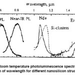
However, at nanometric dimensions silicon exhibits sizable nonlinear effects.1 The idea of exploiting Si for light-emitting devices is appealing because it leads to the possibility of fabricating light-emitting devices compatible with Si-based optoelectronic integrated circuits. The discovery of visible PL at room temperature from electrochemically etched porous silicon has prompted enormous interest in nanocrystalline silicon (NC-Si) structures for their possible applications in optoelectronic integration.1-5 Most of the present day research for photonic applications of Si is directed to develop Si-based nanomaterials that emit light in the visible range efficiently and predictably. It is believed that light emitting Si-devices would not only be cheaper than those made of compound semiconductors and could also be integrated onto traditional circuits. The room temperature PL spectra are shown in Fig. 1.
Figure 1: Room temperature photoluminescence spectra as a function of wavelength for different nanosilicon structures
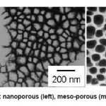
Silicon nanoclusters (porous as well as nano-crystallites) have been the subject of many experimental and theoretical investigations for nanoscale fabrication and miniaturization of microelectronic devices. Porous Si is made up of interconnected branches of nanometer size Si nanocrystals embedded in an amorphous matrix, which can be described in terms of quantum wires and dots. At present there is a common understanding that nanometer sized Si clusters have much different physical and chemical properties from that of bulk Si. Recently, some efforts have been made to build silicon nanotubes or nanowires as well as stable Si quantum dots based on the silicon clusters.4-18 Depending on the sizes of pore diameter p-Si is classified as nanoporous (pore size less than 5 nm), meso-porous (poresize~5-50 nm), and micro-porous (greater than 50 nm) as shown in Fig. 2.
Figure 2: Different p-Si structures: nanoporous (left), meso-porous (middle) and macro-porous (right)
Techniques like plasma-assisted chemical vapor deposition, size-selected cluster deposition, sputtering, laser ablation, electrochemical anodization of Si in HF electrolyte, and ion implantation into matrices have been invented to produce NC-Si. There are many forms of NC-Si and porous Si in particular has attracted special attention due to its easy processing. Structural studies of porous Si showed that it is composed of Si-NS in the forms of columns and clusters.5-7 The structures of Si clusters, especially for small Sin (nd£ 7) have been well determined by Raman and infrared spectroscopy. The geometrical and electronic structure of the larger clusters (n>8) has also been studied theoretically.8 The shape of the larger Sin (ne³20) clusters has been obtained by measuring the nobilities for their ions.9-16 To examine the reactivity of low-dimensional Si structures, experiments have been performed with pure silicon clusters or bare surfaces with ethylene, acetylene, water, ammonia, hydrogen, and oxygen respectively.10 Recently, Park et al.,11 have observed efficient visible PL from amorphous Si quantum dots. It is suggested that, by controlling the sizes of such dots, it is possible to achieve PL over the range of visible light including red, green, and blue.
There are many different characterization techniques presently used to gather information on Si-NS. A combination of Auger, Raman, IR, EXAFS, XPS, AFM, TEM, SEM, EPR, XRD, PL excitation, and linear and nonlinear (Z-scan) optical measurements yields most important experimental results.14-16
Porous Si has proved to be one of the most promising candidates in regard to luminescence among all other Si-based material studied so far. It was the first and it is still the least expensive material using, which the optical properties of Si-NC are studied. The fabrication procedure for p-Si is very flexible. It can be fabricated in multi-layer structures, bi-dimensional arrays (called macro-pores), and straight tubular holes with very high aspect ratios. Both multi-layers and macro-porous Si have provided a cheap way to fabricate large structures with, respectively, one and two-dimensional periodicity in the dielectric properties. These structures can present photonic band gaps (PBG) also called photonic crystals, in which the index of refraction is periodic function of space.12
Porous Si emits light at room temperature in the visible range with quantum efficiencies as high as 10% (one photon emitted for every 10 photo-generated electron-hole pairs). During last few years, several strategies are employed to overcome many limitations, optical gain is demonstrated, and as a result of that present-day Si LED is only a factor of ten away from the market requirements. Silicon nanotechnology played a primary role in these achievements. Today, it is possible to grow several tens and even hundreds of different p-Si layers on top of each other; aperiodic p-Si multi-layer structures can be used to study the effects of disorder on the propagation of light. Under some critical conditions (limit of Anderson localization) the photon diffusion constant vanishes and localization of strong electromagnetic field inside limited volumes of Si is possible. This effect of localization of photons can be exploited for nonlinear optics at low power.16-18
This paper consists of three sections: the first section regards optical properties of nanosilicon in general and photoluminescence mechanism in Si-NS in particular; the second one discusses their applications. The last section concludes the paper by putting all the research efforts so far in this field into prospective and future possibilities.
Optical Properties of Nanosilicon
Porous Si exhibits efficient room temperature luminescence in the visible range.1 The spectrum has three main features: a blue band, the broad red-orange band and an infrared band peaked roughly at 1eV. The blue band is due to emitting centers in the amorphous matrix. Its intensity and peak position are sample dependent. The infrared band is due to the recombination of charge carriers trapped in the dangling bonds at the surface of the nanocrystals. The mechanism responsible for red-orange one is still a matter of debate.
The complexity in the structure of this material has led to the formulation of many different models to explain luminescence. Porous Si is a disordered system consists of an intricate network of crystallites with varying sizes and shapes as well as microscopic dangling bonds and voids. The large surface of such nanometer size objects supports hydrogen and oxygen complexes.5,12-13 Constructing a global theory for the PL spectrum accounting all levels of disorder is an impossible task because of the use of large set of parameters whose numerical values are not accessible by any means (microscopic theory or experiment).
Presently, although detailed understanding of the PL has yet to be achieved but the debate is now focused upon four main models, the quantum confinement, surface states, defects in the oxides, and specific chemical species (siloxenes, etc.). A large amount of experimental evidence has been gathered in favor of the QC model in which short range crystallinity, passivation, and dangling bond defects and distortion play substantial role. It is found that with increasing porosity (decreasing nanocrystals size) the band gap become wider.
PL is studied on two different categories (hydrogen or oxygen terminated surfaces) of Si-NC. For H-terminated p-Si there is a continuous shift of PL peak energy to the visible region from the bulk band gap. On the other hand the PL spectra for oxygen-terminated p-Si are confined to a specific region. The PL spectra progressively shift from red towards blue region with decreasing Si-NC size. It is believed that QC raises the band gap and the PL originates from transitions between the band edges, and the interface state models, where carriers are first excited within the Si-NC, then relax into interface states and radiatively recombine there.
The ensuing research efforts have placed emphasis on the electronic and optical properties of Si-NC. Now PL is used as a standard technique to examine the nanocrystalline nature of these samples although the clear understanding of the PL mechanism has not yet emerged. In fact, there is a long debate concerning the PL mechanisms of porous Si and the Si-NC-embedded Si oxide. For porous Si at least 24 models different from the quantum confinement (QC) model are suggested. These models can be grouped into three categories, namely, (i) quantum recombination model, (ii) surface state model, (iii) molecular recombination model. The first two models agree on the fact that QC plays fundamental role in p-Si luminescence, but they differ in their predictions about the origin. The former model ascribes it to the recombination of excitons within the NC, whereas in the latter individual charge carriers, which could be found either in a bulk NC state (extended state) or trapped in a surface NC state, recombine radiatively. According to the third model, molecular species such as polysilane chains or siloxene rings are present in the amorphous phase of p-Si, and are responsible for the luminescence. The effect of QC is a rearrangement of the energy density of states as direct consequence of volume shrinking in lower dimensions in quantum wells, wires, and dots.10-14
Based on the experimental observations, broadly, two mechanisms have been proposed to explain the observation of enhanced PL in Si-NS. The first suggests that the strong PL in the visible regime is due to the enhancement of the momentum matrix elements associated with the confinement of the electronic wave functions of Si nanoparticles. The second suggests that the surface chemical composition and effects of surface states on band gap to enhance PL. In all these mechanism the size dependent gap energy plays a pivotal role in determining the efficiency of the luminescence. It observed that as the size of the NC reduces the band gap transforms from indirect to direct, which increases the radiative recombination rate via a direct band-to-band recombination process and the band-gap energy is blue shifted in the visible regime owing to the quantum QC effect.12, 13 The QC and a suitable arrangement of interfacial atomic bonds can provide radiative recombination efficiencies that are orders of magnitude larger than in bulk Si, significant nonlinearity, and even optical gain. The trapped-controlled hopping mechanism plays a crucial role in recombination dynamics.
A number of models have been proposed to explain the strong PL in Si NC. The popular viewpoint is the effect of QC in NS with size (d” 5nm), smaller than exciton Bohr radius in corresponding bulk crystal (strong quantum confinement regime). QC enhances the oscillator strength of direct optical transitions in Si crystallites of very high porous Si (70-80%) structures. However, there are number of studies that attributes PL to the emission of different radiative centers on Si-wire surface: the rearranged Si-Si bonds, small hydrogen terminated Si clusters, polysilan complexes, siloxene molecules, defects in Si-oxides, oxygen modified surface states, water molecules with an impurities or some oxygen related chemical species. The possibility of the emission of excitons localized at the Si/SiOn interface is also suggested.18
It is now accepted that for NC having sizes below 5nm due to QC the band gap opens up and the selection rules for radiative transitions gets relaxed. However, QC solely cannot explain the origin of room temperature PL and the role of surface treatments as well as surrounding media are important. The PL peak energy and line shape is dictated by localized surface states or defects in the oxides. These localized states are induced by the structural or compositional atomic disorder at the surface and are energetically placed within the band gap. The surface states exist in the form of self-trapped excitons whose origin is the surface distortion. The surface distortion and disorder induced surface states are intrinsic to NC. Since the surface to volume ratio increases as the crystallite size decreases, the influence of surface states on the PL is highly enhanced for smaller crystallites. Therefore, the origin of room temperature PL is through more than one recombination mechanism in which surface states play a crucial role. The nature of the PL spectra is very much determined by the processing techniques, sample history, and the surrounding media of the NS.
The p-Si luminescence is thought to originate from exciton recombination in quantum dot structures i.e. in the NC. Due to QC effect the exchange energy between triplet and singlet exciton states increases and becomes ~10 meV, which is very large, compare to the value of crystalline Si (~0.1 meV). Recombination from the triplet state is a forbidden transition, with decay times of the order of milliseconds, where as from the singlet state the transition is allowed with decay times in the microsecond regime. The e-h pair decay to the fundamental levels of NC is very fast. At low temperatures the triplet states occupation probabilities are higher than singlet states and that makes the radiative lifetime temperature dependent. Most of the simulation studies e.g., first-principles, Monte Carlo, non-orthogonal tight binding molecular dynamics, effective mass approximation, pseudo potential, density functional theory, generalized gradient approximation, etc. supports QC model. There are many phenomenological models attempts to describe the PL spectra using QC, oscillator strength, exciton contribution, localized surface states, disorder and distortion, relaxation of carriers, gap states due to voids and defects, thermal disorder, distinction of hole and electron contributions, and phonon contribution, etc.10-14
Presently, in addition to the study of linear optical properties there is major interest in nonlinear optical properties of Si nanocrystals for photonic device applications e.g. in all-optical switching. Intensity dependent changes in optical properties e.g. refractive index, third-order nonlinear susceptibility (shown in Fig. 4), and nonlinear absorption are prominent one. It is observed through z-scan technique that the real part of the third order nonlinear optical susceptibility (Re c3 » 1.4 x 10⁻⁹ esu) is order of magnitude higher than the corresponding imaginary part (Im c3 » 0.7 x 10⁻¹⁰ esu). This indicates that the nonlinearity is mostly refractive. The absolute value of c3 is significantly larger than bulk Si value ~ 6.0 x 10⁻¹² esu. This enhancement of c3 in case of low-dimensional structures is attributed to various mechanisms but the effect of QC is the main reason for such enhancement. The higher values of nonlinear absorption in Si-NC compared to that of crystalline bulk Si is due to either multi-photon absorption or saturation of single-photon absorption.16, 18
The optical gain in ion-implanted Si-NC is demonstrated by Bettotti et al.,18 shows that population inversion is possible between fundamental and radiative Si=O interface states. The gain is explained in terms of three-level model and more recent one based on Si-Si dimmer and the self-trapped exciton. Although, there is no global model for gain but it is realized that the interface states play critical role in the optical gain. The race is now open towards achieving Si laser. One of the most promising ways to achieve this target is through rare-earth doped Si-NC, and particularly erbium (Er) is most interesting due to its emission wavelength at 1.54 µm where optical fibers have transparency window.
The effect of QC is also exploited to built Si-lasers using quantum dots, super-lattices, and multi-quantum-well structures. Si laser made of GaAs/AlGaAs quantum well structures for THz emission is also proposed. Quantum parallel laser (QPL) from Ge0.5 Si0.5/Si super-lattice is also designed for near infrared communications operation in the wavelength range 3-5 µm. These lasers at room temperature has gain values are as high as 134 cm-1 for current densities 5000 A/ cm-2. Si-NC deposited by reactive deposition onto fused quartz shows population inversion and amplified spontaneous emission. The Si-NC reconstructed from ultra small sized colloidal nanoparticles also shows population inversion. The luminescence of these particles is dominated by naked-eye visible blue emission at 390 nm. There are basically two time regimes for the luminescence decay in Si-NC: (i) long-lived luminescence decays (~50 µs) and (ii) fast luminescence at 750 nm wavelength that decays in a few nanosecond and disappears at low pumping rates. The fast PL is due to the population inversion at the Si-NC interface states with a very short lifetime for the inversion. From application point of view a fast population inversion is desired that generates short light pulses.
It is important to achieve efficient electroluminescence (EL) in order to employ Si-NS for the production of photonic devices. At present commercial LEDs have external efficiency orders of magnitude higher than Schottky-type p-Si structures. There are many difficulties encountered so far to achieve it and some of them are: El degradation at fast time scale and poor carrier injection due to the presence of highly resistive intricate network in p-Si. The fast degradation is due to the presence of islands in the metal layer as well as due to the decay of light emission itself. There are efforts to improve the EL characteristics by incorporating a micro-cavity within the p-Si LED. The incorporation of such cavity increase the light emission, narrows down the spectral range, and imparts strong directionality of the emitted light. Micro-cavities are characterized by a wavelength region where all the light is reflected and by a resonance wavelength for which the field intensity in the cavity is enhanced. One of the disadvantages of these p-Si micro-cavities is their aging instability. Further investigation is needed to fully characterize these structures and optimize their fabrication.5,14,18
Applications
Recently for photonic applications multi-layer p-Si structures are used to fabricate Bragg reflectors, Fabry-Perot filters and micro-cavities. The fabrication and optical characterization of dielectric p-Si multi-layers with periodic variation of refractive index as a function of depth is possible through etch process.17,18 One can periodically vary the etch parameters e.g. current density, light power, and dope substrates. These complex multi-layers structures are used to create interferential filters and/or narrow band reflectors formed by dielectric films. On the bases of these multi-layers Bragg reflectors and Fabry-Perot devices is fabricated that helps to tune and narrow down the p-emission band. Other application of p-Si multi-layers includes planer wave-guides in infrared and visible region. Commercial applications presently hindered by scattering loss and absorption in the porous medium.
The Fabry-Perot devices help to fabricate p-Si micro-cavities, which act as confinement region for emitted photons and modify the photon density of states that finally lead to alterations of spontaneous emission characteristics. The effect of micro-cavity is manifested in many ways: (i) A 16-fold increase in intensity, (ii) Strong narrowing of emission band, (iii) Decrease in the luminescence decay time constant, and (iv) Strong directional emission from the micro-cavity. These features are evidenced through angular resolved PL measurements and time-resolved excitation spectroscopy.14
Porous Si Schottky diodes have been studied with yielding efficiencies ~10-4. These types of diodes are used to achieve p-Si LEDs with improved performance. The current voltage characteristics proved to be independent of the type of metal used for the electrical contact. Devices based on Si homo-junctions have been fabricated for providing more adequate carrier injection mechanism for efficient EL and slower degradation. Micro-cavity LEDs are very useful to achieve efficient EL. The diodes were obtained from thin film of Au deposits. In 1996 attempt was made to integrate a p-Si LED with Si electronics and it was possible to turn the LED on and off by applying small current pulse to the base of the transistor. Finally arrays of such integrated structures are fabricated.16
The very large value of the surface/volume ratio for sponge porous structures of Si ~ 500 m2 cm-3 makes them highly chemically reactive. This feature of p-Si is exploited for sensors applications to sense humidity, organic molecules, ethanol, nitrous oxide etc. Biosensors based on p-Si micro-cavities are very useful for distinguishing bacteria and viruses because these cavities have strong response to DNA molecules and lipids. Through parametric distinction of physical properties (integrated PL as sensing parameter, refractive, and PL peak) such biosensors are used to measure concentration of polar species.18
Nanosilicon is a good candidate for developing two-dimensional photonic crystals (2D-PC) by anodic electrochemical dissolution method. This method is technologically friendly, simpler, cheaper, and faster and wafer scalable. These 2D-PC made from p-Si has air columns in the Si-matrix that acts as macro-pores. They can be filled with active materials to form either enhanced LEDs or nonlinear media. Another application of p-Si is in fabricating p-Si Fibonacci quasi-crystals. In these structures the localization of light waves helps for many nonlinear applications. The band edge pulse propagation in Fibonacci quasi-crystals is also reported. It is observed that the electric field intensity of optical modes shows local field enhancement effect, which is due to the weak localization of modes. The nature of localization is somewhere in between exponentially localized and that of extended Bloch states. This investigation is very important from fundamental physics point of view as the time resolved propagation measurements on p-Si Fibonacci quasi-crystals demonstrate the presence of localized photon states.16-18
Conclusions
The nanosilicon research field is highly fertile with numerous technological possibilities. It is now believed that the prospects for exploiting nanosilicon for photonics are non-longer poor. With the advent of rapidly growing activities in nanotechnology the optical proper ties (linear and nonlinear) of bulk crystalline Si materials can be changed dramatically by shrinking their sizes into lower dimensions. Inside the integrated circuits the interconnect bandwidth requirements trying to introduce the optical functionality.
The fabrication process had been mastered and controlled with precision. Complex multi-layer structures are available to study photon propagation on disordered structures and light localization. All the results (theory, experiment and simulation) on photoluminescence mechanism strongly support QC effect of exciton recombination. Devices based on silicon homo-junction are recently been created. It is important to achieve efficient electro-luminescence (EL) to employ p-Si for the production of photonic devices. To achieve efficient EL one needs to find an efficient method to supply charge to the p-Si layer. There are two aspects: maximization and stabilization of light emission. Homo-junction devices and incorporation of micro-cavities may be the possible solution to fulfill these aspects. However, this field requires more work to be done although first p-Si based photonic device is commercially available.
In last few years Si photonic band-gap materials, optical gain in Si-NC, Si LED and Si-based optoelectronic devices are demonstrated in nanoporous and macro-porous Si through inexpensive fabrication techniques. The main issue at present is the difficulty of large-scale production of p-Si with controlled growth and stability over time as demanded for the device applications. The worldwide technological race is now to achieve all Si-based integrated photonic circuits called the system-on-chip (SoC) approach.
Acknowledgements
SKG is indebted to Prof. K.P. Jain (IIT, Delhi), and Prof. Sir Roger Elliott (Oxford University) for introducing in this field and also educating with many critical concepts. SKG and HST specially thank to the Physics Department, Addis Ababa University for providing all facilities to complete this work.
References
- L.T. Canham, Appl. Phys. Lett., 57: 1046 (1990).
- V. Lehmann and U. Grunin, Thin Solid Films, 297: 13 (1997).
- Y. Kanemitsu, Physics Reports, and references therein. 263: 1 (1995)
- J. Lin, G.Q. Yao, J.Q. Duan and G.G. Qin, Sol. State Comm., 97: 221 (1996).
- L. Pavesi and R. Guardini, Braz. J. Phys., 26: 151 (1996).
- T. Takagahara, Phys. Rev. B., 47: 4569 (1993).
- M.S. Hybertsen, Phys. Rev. Lett., 72: 1514 (1994).
- L.W. Wang and A. Zunger, J. Phys. Chem., 98: 2158 (1994).
- L.W. Wang and A. Zunger, J. Chem. Phys, 100: 2394 (1994).
- P. Vasiliev, S. Ogutt and J.R. Chelikowsky, Phys. Rev. Lett., 86: 1813 (2001).
- N.M. Park, C.J. Choi, T.Y. Seong and S.J. Park, Phys. Rev. Lett., 86: 1355 (2001).
- S.K. Ghoshal, U. Gupta, and K.S. Gill, Ind. J. Pure & Appl. Phys., 43: 188 (2005).
- S.K. Ghoshal, K.P. Jain and S.R. Elliott, J. Metast. & Nanocryst. Mat., 23: 129 (2005).
- L. Pavesi, L. D. Negro, C. Mazzoleni, G. Franzo, and F. Priolo, Nature, 408: 440 (2000).
- L. Liu, C.S. Jayanthi, and S.Y. Wu, J. Appl. Phys., 90: 4143 (2001).
- S. Viajayalakshmi, A. Lan, Z. Iqbal, and H. Grebel, J. Appl. Phys., 92: 2490 (2002).
- M.V. Wolkin, J. Jorne, P.M. Fauchet and C. Delrue, Phys. Rev. Lett., 82: 197 (1999).
- P. Bettoti, M. Cazzanelli, L. Dal Negro, B. Danese, Z. Gaburro, C. J. Oton, G. Vijaya Prakash and L. Pavesi, J. Phys.: Cond. Mat.,14: 8253 (2003).

This work is licensed under a Creative Commons Attribution 4.0 International License.