Study of Electrical Optical and Structural Properties of Lead Selenide Sulphide Ternary Thin Films
S. R. Jadhav1 and U. P. Khairnar2
1Department of Physics, Rashtriya College, Chalisgaon, Dist- Jalgaon - 424 101, India.
2Department of Physics, S.S.V.P.S. ACS College, Shindkheda - 425 406, India.
Corresponding Author E-mail: upkhairnar@rediffmail.com
DOI : http://dx.doi.org/10.13005/msri/070213
Article Publishing History
Article Received on : 04 Oct 2010
Article Accepted on : 12 Nov 2010
Article Published :
Plagiarism Check: No
Article Metrics
ABSTRACT:
Polycrystalline Lead Selenide Sulphide thin films have been deposited on glass substrate at 300 K by thermal evaporation technique. The different sets of samples of varying composition 'x' from 0.1 to 0.9 were deposited and annealed at reduced pressure of 0.1 micron for duration of 4 hours at temp (373) K. The material parameters determined are bulk resistivity 1.450 (Ohm-cm), mean free path 2820Å and carrier concentration 5.5 x 10¹² per cm3. The estimated activation energy for heating cycles is larger as compare to cooling cycles. Fermi-energy determine from TEP study are within ranges between band gap energy and activation energy values.
Also the XRD study reveals that all the samples were polycrystalline having cubic FCC, cubic and tetragonal structure. The dependence of absorption coefficient ‘α’ on photon energy has been determined. The analysis of result so that for Lead Selenide Sulphide films of different composition, direct transition occurs with band gap energy in the range of 1.0 eV to 1.4 eV. Refractive indices and extinction coefficient have been evaluated and are in the range 1.20 to 4.80 and 0.005 to 0.0245 respectively. The compositions of films were analyzed using Energy Dispersive X-ray Analysis (EDAX). Also the grain size is determined from X-ray diffraction study. Most of the grain sizes are below 300 Å indicates that the film material exhibits nano structure. The SEM analysis indicates that the film is covered with large number of star shaped microgranuals. The size of the microgranuals increases with increasing ‘x’.
KEYWORDS:
Thermal evaporation; Optical constants; XRD; EDAX; SEM
Copy the following to cite this article:
Jadhav S. R, Khairnar U. P. Study of Electrical Optical and Structural Properties of Lead Selenide Sulphide Ternary Thin Films. Mat.Sci.Res.India;7(2)
|
Copy the following to cite this URL:
Jadhav S. R, Khairnar U. P. Study of Electrical Optical and Structural Properties of Lead Selenide Sulphide Ternary Thin Films. Mat.Sci.Res.India;7(2). Available from: http://www.materialsciencejournal.org/?p=2397
|
Introduction
A series of new materials of varying chemical and physical properties could be obtained by varying the composition of constituents of binary and ternary semiconductors; in this respect for example newer materials like Pb1-x CdxS, CuInS2, CuInSe2, ZnSSe/ZnSe and ZnCdS can be used for better efficiency.1-7 Sulfide and mixed sulfide thin film coating find extensive use in number of electronic devices such as photoconductors, thin film transistors, photo-detectors, electroluminescent cells and photovoltaic devices.8-12 Lead sulfide thin films have been deposited by LP-MOCVD and AACVD, using single-source precursors of the type [Pb(S2CNRR’)2]. The same class of compounds for the preparation of nanocrystallites and thin films of PbS/Se has been studied.13-15 Continuous variation of the energy gap (and other properties), which can be obtained by varying the relative concentration of constituent elements in mixed and alloyed ternary semiconductor compounds has been extensively used to tailor the spectral response of detectors for opto-electronic applications. The aim of this paper is to investigate the effect of composition of ternary solid thin films. However mixed and alloy selenides are rarely studied. Keeping this in mind thin films of (PbSe)x (PbS)1-x type are prepared and characterized in the present work.
Material and Methods
For the preparation of ternary compound semiconductors (PbSe)x(PbS)1-x the constituent compounds PbSe and PbS have been taken in molecular stiochiometry proportional weights and crushed and mixed homogeneously. The different sets of samples of varying compositions (x = 0.1 to 0. 9) were deposited on to the amorphous precleaned glass substrates at room temperature 308 K. All the samples are deposited under the similar optimized conditions. The thicknesses of films were controlled by using quartz crystal thickness monitor model No. DTM-101 provided by Hind-High Vac. The deposition rate was maintained 10-15 Å/ sec constant throughout sample preparations. These samples were annealed at reduced pressure of 0.1 micron for the duration of 4 hours at the temperature of 373 K and maintained carefully. These samples were then used for different characterizations.
The structural characterization was done by X- ray diffractometer (Rigacu-Miniflex, Japan) with CuKa radiation (1.5418Å) and Analytical Scanning Electron Microscope (SEM) JEOL JSM 6360 (LA), with EDAX attachment. The transmittance of the films was determined at normal and near normal incidence of light in the wavelength range 200 to 2600 nm by means of double beam spectrophotometer (Hitachi-330 model).
Results and Discussion
Electrical Properties
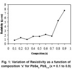
Resistivity variation as a function of composition parameter ‘x’ as presented in Fig.1 Seems to be obvious as resistivity of pure material (i.e. x = 0) PbS and PbSe are of value 0.027 W-cm and 0.25 W-cm respectively. As x increases resistivity should increase and it should be maximum at x = 0.5, theoretically instead of this it is observed that resistivity increases slowly with x up to x = 0.7 and then it rapidly increases up to x = 0.9 For all samples x ¹ 0 the resistivity is larger than that of pure material films of same order of thickness around 2000Å.13 Similar behavior of resistivity variation for all composition of ‘x’ may be due to similar processes of activation of conductivity of charge carriers may be involved. This behavior in the resistivity is supported by different structural phases involved as composition parameter ‘x’ increases. And similar observations have observed by Deshmukh et. al.16 In this study of (CdSe)x– (PbS)1-x composite thin films.
Figure 1: Variation of Resistivity as a function of composition ‘x’ for PbSex PbS1-x (x = 0.1 to 0.9)
Material parameters evaluated approximately were bulk resistivity r0 = 1450 × 10-3 W-cm, mean free path l0 = 2820Å and carrier concentration n = 5.5×10¹²/cm3. The carrier concentration evaluated seems to be very low value as compared to the reported value of 1018/ cm3 by Fujita et.al.17 for PbS0.5 Se0.5 prepared by co-evaporated method on rock salt and PbSx Se1-x single crystal substrates.
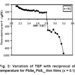
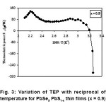
For all compositions change in thermoelectric power at low temperature end is appreciably larger and very small changes at high temperature region except the compositions PbSe0.3 S0.7, PbSe0.4 S0.6 and PbSe0.5 S0.5, have appreciable thermoelectric power changes over entire temperature range may be increasing or decreasing. From the Fig. 2–3 fermi energies have been evaluated from the linear variation of thermoelectric power verses reciprocal of temperature. These values are within ranges in between band gap energy values around 1.2 eV and evaluated thermally activation energies (0.24 – 0.44) eV.
Figure 2: Variation of TEP with reciprocal of temperature for PbSeX PbS1-x thin films (x = 0.1)
Figure 3: Variation of TEP with reciprocal of temperature for PbSeX PbS1-x thin films (x = 0.9)
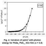
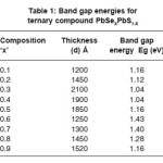
characteristic feature as a function of wavelength. Few samples are opaque below 750 nm and some of them are opaque below 950 nm. Then the transmittance increases linearly and rapidly with wavelength and attains maximum value. Also in few samples there is a well defined maxima and minima peak from the spectra. The transmittance data have been used to calculate absorption coefficients an attempt is made to plot the curves (ahn)2 vs hn and the curve is presented in Fig. 4. All the compositions curves shows linear variations and extended line intersects the hn axis. This intersection gives optical band gap energies. These evaluated values are presented in Table 1. These values are in the range 1. 04 – 1.43 eV and varied randomly when composition parameter is less than 0.5 (x < 0.6). Band gap energy ‘Eg’ is maximum for x = 0.6 and it decreases at x > 0.6, for these samples the thickness is also of increasing order and therefore band gap energy is also as expected goes on decreasing order. This fact is also explained for PbSe and PbS films.18-21
Figure 4: Variation of (ahn)2 with photon energy for PbSex PbS1-x thin film (x = 0.8)
Table 1: Band gap energies for ternary compound PbSeXPbS1-X
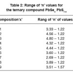
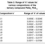
The observed transmittance at normal and near normal incidence and reflectance at near normal incidence data have been used to determine the optical constants refractive indices ‘n’ and extinction coefficient ‘k’. The range of ‘n’ and ‘k’ values for all the samples of different composition of parameter ‘x’ are presented in Table 2 and 3 respectively and are in the range 1.20 to 4.80 and 0.005 to 0.0245 respectively.
Table 2: Range of ‘n’ values for the ternary compound PbSex PbS1-x
Table 3: Range of ‘k’ values for various compositions of the ternary compound PbSex PbS1-x
Structural Properties
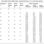
Table 4 represents the detail EDAX analysis of the composition of starting basic ingredients and film composition comparisons. And compares expected atomic percentage and actual atomic percentage in the film material for all the samples of all compositions ‘x’ varying from 0.1 to 0.9.
Table 4: EDAX Data for (PbSe)x (PbS)1-x Composite thin films (x = 0.1 to 0.9) (atomic percent)
It is seen from this table that the samples of compositions x = 0.3, 0.4 and 0.5 are not much deviated from the expected atomic percentage while the samples with x = 0.6, 0.8 and 0.9 are comparatively more deviated than expected. While the sample of composition x = 0.7 is largely deviated from the expected atomic percentage.
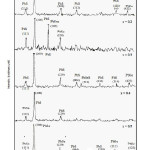
The XRDs of all compositions (0.1 ≤ x ≤ 0. 5) have been presented in Fig. 5. X-ray diffractograms differs for different compositions in relative intensities, angular positions and even relative orientations. The comparison of observed and standard diffraction parameters for three different structures of PbSeS, PbSe and PbS compounds. A detailed comparison indicates that observed and standard ‘d’ values very closely agree with each other for all composition parameters x varying from 0.1 to 0.9. The XRD analysis confirms that film material is polycrystalline for all compositions.
Figure 5: X – Ray Diffractograms of various (PbSe)x (PbS)1-x Structures (x = 0.1 to 0.5)
The relative intensities of prominent reflections of cubic structures of PbSe and F.C.C. structure of PbS (111) (200) and (220). From this table it is observed that, as the compositional parameter x increases, the orientation of crystallites changes from (200) of face centered cubic of PbS to (200) cubic of PbSe.
From the analysis of XRD it is found that the films are of composite structure of PbSe, PbS and PbSeS i.e. cubic face centered, cubic and tetragonal structures. In other words this analysis of different peaks indicating the presence of phases, cubic PbSe, face centered cubic of PbS as well as tetragonal of PbSeS. It is interesting to note that for x=0.1 – 0.2 face centered cubic face of PbS is prominent than phases of PbSe and PbSeS. For x=0.4 and 0.5 films are only phase of cubic PbSe and F.C.C. of PbS for x = 0.6 and 0.8 films are constituting all the three phases prominently. For x=0.9, the films are constitutes tetragonal and cubic phase only, for x = 0.7, the film material is of prominent cubic phase of PbSe only.
In general it may be concluded that film materials of various compositions parameters are of polycrystalline, composite of different phases and having relative crystalline orientation along (200) the samples. This may be due to the effect of WD changes from 9.3 to 9.6.
As the percentage of PbSe increases the size of the microgrannuals also increases without any sort of orientation and regularities. But when the concentration of PbSe is increased to 80 (x = 0.8) some granules are turn onto sphearolytic shape with the fibers at the top of the surface. The fibers on the spheroids are clearly visible, when the x value increased from 0.8 to 0.9. The size of spheroids in some cases have been increased as compare to x = 0.8. But when x = 0.8 then numbers of spheroids is large as compare to x = 0.9 and also their shape is more regular. So for the dendraitic growth of the film is suitable at x = 0.2 (PbSex PbS1-x), but when same film required at sphearolytic shape then x = 0.8 (PbSex PbS1-x) is suitable.
From this we conclude that for x = 0.2 gives the film of dendraitic growth and for x = 0.8 gives the film of sphearolytic shape. Both are in crystalline form and x = 0.2 and x = 0.8 both are having the good quality of the mixed ternary films.
Thin films of Polycrystalline Lead Selenide Sulphide were prepared by the thermal evaporation technique.
Estimated activation energy for heating cycles is larger as compared to cooling cycles. Also for x < 0.5 the activation energies are of higher magnitudes as compare to x > 0.5.
The Estimated values of Fermi-energy determined from thermo electric power study are within ranges between band gap energy and activation energy values.
The Band gap energy varies randomly when x < 0.5 and it is systematically decreases when x > 0.6.
Detailed X-ray diffraction study reveals that the films are of composite structure i.e. Cubic fcc, Cubic & Tetragonal.
Most of the estimated grain sizes are below 300Å. This indicates film material exhibits nano-structure.
SEM analysis indicates that the film is covered with large number of star shaped microgrannuals, the size of the microgrannuals increases with increasing ‘x’ when x = 0.8 the microgrannuals are turn on to regular sphearolytic shape and when x = 0.2 film shows dendraitic growth.
Acknowledgements
The authors are thankful to Prof. Dr. P. H. Pawar, Principal, Z. B. Patil College, Dhule. The authors are also grateful to Prof. Dr. P P. Patil, Director and Head, Department of Physical Sciences, North Maharashtra University, Jalgaon.
References
- J.J.Loferski, “Proc. workshop photovoltaic conversion of solar energy for terrestrial application” 1, 27 sponsored by National Science Foundation (USA, 1973).
- A.K.Sood, K.Wu. and J.N.Zemel, Thin Solid Films, 48: 73 (1978).
- J.D.Jenes and R.B.Schoolar, Electron. Mater., 7: 237 (1978).
- A.R.Calwa, J.A.Mroczouski and T.C.Harman, J. Electron Mater., 1: 191 (1972).
- P. Stitu., Phys. Status Solidi, A15: K19 (1973).
- Ozden Akinci, H. Hakan Gurel and Hilmi Unlu, Thin Solid Films, 517: 2431 (2009).
- Bhaskar Kumar, Parag Vasekar, Shirish A. Pethe, Neelkanth G. Dhere and Galymzhan Koishiyev, Thin Solid Films, 517: 2295 (2009).
- G. Gordillo, Solar cells, 14: 219 (1985).
- G.B. Reddy, D.K. Pandya and K.L.Chopra, Solar Energy Mat., 15: 235 (1987).
- J.A.Rodriguer and G. Gordillo, Solar energy Mat., 19: 421, (1989).
- P.K.Nair, M.Ocampo, A. Fernandez and M.T.S.Nair, Solar Energy Mat., 20: 235 (1990).
- G.C. Morris and R.Vanderveen, Solar Energy, Mat. Solar Cells, 26: 217 (1992).
- T. Trindade and P. O’Brien, Chem. Vap. Deposition, 3: 75 (1997).
- N. I. Fainer, M. L. Kosinova, Y. M. Rumyantsev, E. G. Salman and F. A. Kuznetsov, Thin Solid Films, 280: 16 (1996).
- L.I. Maissel and R. Glang, “Hand Book of Thin Film Technology, Mc Graw – Hill, Book Co. New York, (1970).
- L.P. Deshmukh, B.M.More, S.G. Ghollkatti and P.P. Hankare, Bull. of Mat. Sci., 17: 455 (1994).
- Fujita shigeo, Ozaki Hideyuki and Shiosaki Tadashi Akira, Shinku, 20(12): 412 (1977).
- T.H. Mayers, S.W. Edwards and J.F. Schetzina, J. Appl. phys., 52: 4231 (1981).
- N.El. Kadry, M.F. Ahmed and K. Abdel Hady, Thin Solid Films, 274: 120 (1996).
- F. Cerdeira, I.T. Torriani, P. Mostisuke, V. Lemos and F. Decker, Appl. Phys, A 46: 107 (1988).
- R.F.C. Farrow, G.R. Jones, G.M. Willams and I.M. young, Appl. Phys. Lett., 39: 954 (1981).

This work is licensed under a Creative Commons Attribution 4.0 International License.