Preparation of Zno Film on P-Si Substrate by Silar and Heterojunction Characteristics of P-Si/N-Zno
P. Mitra
Department of Physics, The University of Burdwan, Golapbag, Burdwan - 713104, India.
DOI : http://dx.doi.org/10.13005/msri/080128
Article Publishing History
Article Received on : 03 Jan 2011
Article Accepted on : 08 Feb 2011
Article Published :
Plagiarism Check: No
Article Metrics
ABSTRACT:
Zinc oxide (ZnO) thin films was deposited on p-silicon (Si) substrate from ammonium zincate bath following a chemical dipping technique called SILAR. Structural characterization by X-ray diffraction (XRD) indicates the formation of polycrystalline single phase ZnO with strong c-axis orientation. I-V characteristic of the p-Si/n-ZnO heterojunction was studied and rectification was observed. The maximum value of forward to reverse current ratio at room temperature was ~15 at 3.0 V. It increases to ~30 at 100oC.
KEYWORDS:
p-Si/n-ZnO heterojunction; C-axis orientation; I-V characteristics
Copy the following to cite this article:
Mitra P. Preparation of Zno Film on P-Si Substrate by Silar and Heterojunction Characteristics of P-Si/N-Zno. Mat.Sci.Res.India;8(1)
|
Copy the following to cite this URL:
Mitra P. Preparation of Zno Film on P-Si Substrate by Silar and Heterojunction Characteristics of P-Si/N-Zno. Mat.Sci.Res.India;8(1). Available from: http://www.materialsciencejournal.org/?p=2581
|
Introduction
ZnO films have been epitaxially grown on sapphire or Si substrates by several physical and chemical methods such as molecular beam epitaxy (MBE), sputtering, MOCVD and sol-gel.1-3 Silicon is suitable for the integration of optoelectronic devices. It is also cheaper and easier to cleave silicon compared to sapphire. Thus efforts have been mostly directed to grow n − ZnO thin films on substrate. Heterojunction of np−ZnOSi/p –Si have potential applications in the visible and ultraviolet photodiodes, gas sensors among many others.3, 4-5 In this paper, n-ZnO films were grown on p-Si substrates by successive ion layer adsorption and reaction (SILAR). The structural properties of ZnO films deposited on silicon substrate were evaluated. The heterojunction properties were also investigated by means of I–V measurements at different temperatures.
Earlier we reported the preparation of ZnO thin films by this technique from sodium zincate or ammonium bath.6-8 Since SILAR has the advantage that films can be deposited on any kind of substrate, the objective of the present work was to promote Interest in this method as applied to fabrication of ZnO thin film on p-Si substrate. The microstructural features of the films were studied using X-ray diffractometer (XRD). Characterization of the heterojunction so formed was carried out by current-voltage measurements. The I-V characteristics of the n-ZnO/p-Si heterojunction was measured in a Solatron meter (Schlumberger S1 1286).
Experimental
Material and Methods
The details of zinc oxide film deposition on microscope glass substrate following chemical dipping from sodium zincate or ammonium zincate bath have been reported elsewhere.6-8 In brief, the process involves multiple dipping of the substrate in the zincate bath maintained at room temperature and hot water bath maintained near boiling point. The zincate complex was prepared by adding sodium hydroxide (NaOH) or ammonium hydroxide (NH4OH) in a solution of zinc salt (zinc sulphate or zinc acetate).
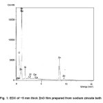
Dipping of the substrate in zincate bath results in a thin layer of the zincate solution on the substrate. Subsequent dipping of the substrate in hot water leads to breaking down of the complex and formation of ZnO. For the present work, ammonium zincate bath was selected. Although the growth rate from sodium zincate bath (0.20 per dipping per mole) is always on the higher side compared to that from ammonium zincate bath (0.16 per dipping per mole), there is incorporation of sodium in films prepared from sodium zincate bath. Figure 1 shows the energy dispersive X-ray (EDX) pattern of an ~5.0 mm thick ZnO film obtained from sodium zincate bath on silicon substrate. The peak due to sodium merges with one peak of zinc. Sodium was found to be present in approximately 0.7 element %. Trace amount of Ca (~0.11 atomic %) and Cl (0.06 atomic %) was also detected in the film.
The silicon (p-Si) substrate used for deposition was first dipped in the zincate bath and then in hot water (maintained near boiling point). The dipping time in each bath was 2 seconds. The film thickness, measured gravimetrically was ~2.2 µm after 100 dipping in the two baths. The silicon substrate [p-Si (100)] used for deposition was etched in dilute hydrofluoric acid (HF) to remove native oxide. It was then thoroughly washed with distil water followed by cleaning with 1:1 by volume methanol-hydrochloric acid mixture and finally followed by deionized water cleaning. The deposited ZnO films were subsequently annealed in air at 200oC.
Figure 1: EDX of ~5 mm thick ZnO film prepared from sodium zincate bath
Results and Discussions
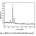
Figure 2 shows the X-ray diffraction (XRD) pattern of a ~2.2 µm thick ZnO film deposited on silicon substrate from ammonium zincate bath. It is seen from fig. 2 that (002) is the strongest line, indicating strong preferred c-axis orientation. The other peaks at (100) and (101) are in agreement with JCPDS.9
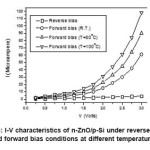
The heterojunction characteristic of was measured by studying the characteristics. Prior to this, room temperature curing silver paste was applied on ZnO and aluminum dots were evaporated on silicon in a vacuum coating unit. Silver and aluminium are known to form ohmic contacts on ZnO and Si. Figure 3 shows the characteristics of heterostructure at different temperatures. The reverse current increases linearly with the increase of the reverse bias voltage which can be explained by the generation current in the depletion region.3 The forward current increases nonlinearly with forward bias voltage. Thus the junction was found to be rectifying and the turn-on voltage is about 1.5V. The maximum forward-to-reverse current ratio was found to be about 15 at room temperature. This is on the lower side of that normally reported5,10 While Basu et al.,5 have reported a forward to reverse current ratio of 80 at 1V; Ajishma et al.,10 reported a value of 1000 at 5V for n-ZnO/p-Si heterojunctions. While Basu et al.,5 deposited ZnO films on p-Si substrate by chemical vapor deposition (CVD) technique, Ajishma et al.,10 prepared ZnO films by pulsed LASER deposition technique. The value of ~15 obtained for the present case is possibly due to very high resistivity of SILAR deposited films7 compared to other techniques. With increasing temperature, the forward-to-reverse current ratio increases and it becomes ~30 at 100oC. Still higher temperatures could not be measured due to use of room temperature curing Ag paste.
Figure 2: XRD of ~2.2 mm thick ZnO film on p-Si
Figure 3: I-V characteristics of n-ZnO/p-Si under reverse bias and forward bias conditions at different temperatures
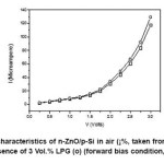
Figure 4: I-V characteristics of n-ZnO/p-Si in air (¡%, taken from figure 3) and in presence of 3 Vol.% LPG (o) (forward bias condition, T=100oC)
Conclusions
An analysis of the results presented here indicates that n-ZnO thin films can be successfully grown on p-Si substrates by low temperature SILAR technique. The films have high preferred c-axis orientation. Current-voltage (I–V) characteristics of n-ZnO/p-Si heterojunction exhibit nonlinear and rectifying characteristics with maximum forward to reverse ratio of ~15 at 3.0 V at room temperature. The low value of forward to reverse current ratio is due to high resistivity of SILAR deposited films. The current ratio increases to ~30 at 100oC. The structure is weakly sensitive to LPG at this temperature.
References
- Y. I. Alivov, U. Ozgür, S. Doðan, D. Johnstone,V. Avrutin, N. Onojima, C. Liu, J. Xie, Q. Fan, H. Morkoç and P. Ruteran, Superlattices & Microstructures, 38: 439 (2005).
CrossRef
- J. Skriniarova, J. Kovac, D. Hasko, A. Vincze, J. Jakabovic, L. Janos, M. Vesely, I. Novotny, J. Bruncko, Journal of Physics: Conference Series 100: 1-4 (2008).
CrossRef
- Y. Zhang, D. Guotong, B. Zhang, Y. Cui, H. Zhu and Y. Chang, Semicond. Sci. Technol., 20: 1132 (2005).
CrossRef
- J. Y. Lee, Thin Solid Films, 403-4: 553 (2002).
CrossRef
- S. Basu and A. Dutta, Phys. Stat. Sol.(a),136: 267 (1993).
CrossRef
- Mitra and H. S. Maiti, Sensors and Actuators, 97: 49 (2004).
CrossRef
- Mitra and J. Khan, Materials Chemistry and Physics, 98: 279 (2006).
CrossRef
- Mondal, K. P. Kanta and P. Mitra, J. Phys. Sc. , 12: 221 (2008).
- L. G. Berry (ed.) “Powder Diffraction File”(JCPDS, Philadelphia, 1960) Card No. 5-0664.
- R. S. Ajimsha, M. K. Jayaraj and L. M. Kukreja, Journal of Electronic Materials, 37:770 (2007).
CrossRef

This work is licensed under a Creative Commons Attribution 4.0 International License.