Introduction
Carbon dioxide is one of the most frequently found nontoxic gases in atmosphere. The CO2 gas is odorless & cannot be detected without measuring instruments. CO2 is harmless in small quantity because it is naturally consumed by the soil, trees and the ocean. However, the concentration of CO2 is increasing in the atmosphere due to industrial revolution, combustion process and green house effect. This increase in concentration may lead to problems in future as in high concentrations it is fatal & insidious. Therefore, demand for the detection of carbon dioxide gas is increasing for global environmental surveillance and in several key fields such as indoor and outdoor air quality monitoring, biogas, smoke systems, process control in fermentation, medical field and vegetable intelligent packaging. Variety of materials like semiconductors, polymers, and zeolite based materials are being used as CO2 gas sensors.1-4 Most of the recently available carbon dioxide sensors work on optical principles and are usually bulky and expensive. Therefore, there is a need of an alternative sensor for CO2 monitoring which is not only cheap but also efficient. In this context, use of semiconductor metal oxides for carbon dioxide detection is an excellent option due to their low power consumption, cost effectiveness, efficiency, ability to integrate into electronic and control devices and response to gases after exposure.5-8
Zinc oxide (ZnO) is one of the unique and promising metal oxide semiconducting materials with attractive optical and electrical properties. It is an n-type semiconductor of wurtzite structure with a direct energy wide-band gap of about 3.37 eV and a relatively large excitation binding energy of 60 meV at room temperature.9 It can be used as a transparent electrode in solar cells and flat panel displays as well as for the fabrication of gratings in optoelectronic devices, as a window material in antireflection coatings and in optical filter.10-11 Furthermore, ZnO is being widely used as a gas sensor due to its conductivity changes when exposed to gases because of its chemical sensitivity to gases, suitability to doping, non-toxicity, and low cost, high chemical and mechanical stability, eco-friendly nature, biocompatibility and abundance.12-13
Review of literature reveals that lot of work has been carried out on ZnO material as a gas sensor for sensing ethanol, ammonia, hydrogen, methane, nitrogen, oxygen, carbon monoxide, & hydrogen sulphide gases.12,14-30 However, very meager work has been carried out on CO2 gas sensor. Zinc oxide thin films, synthesized using reactive d.c. sputtering method, have been used for gas sensor applications and the sensitivity of the film synthesized at substrate temperature of 130°C is found to be 2-17 in the presence of CO2 gas at a measuring temperature of 100°C.31 The study on the response of ZnO tetrapod-based sensor in various gas environments such as H2, CO, i-butane, CH4, CO2, and SO2 at room temperature is also carried out.29 Nevertheless, the gas sensor based on pure ZnO can not cope up with current requirements for fast, continuous and trace detection. Attempts have been made to improve the properties of gas sensors by using additives like noble metals and transition metals32-34 and there is lot of scope and need for the improvement of gas sensitivity. From this point of view, swift heavy ion (SHI) irradiation is one of the effective techniques which can alter the material properties to a great extent. However, the interaction of an ion beam with a material depends on the ion energy, fluence and ion species,35-36 While traveling through the matter, swift heavy ions lose their energy due to interaction with target atoms through inelastic collision. This energy released in a very short duration of time leads to amorphisation, recrystallization or phase change. Moreover, it is reported in the literature that the H2S gas sensitivity of the ZnO nanowires could be modulated and enhanced by He+ implantation at an appropriate dose.37 Effect of 100 MeV O7+ ions irradiation on ethanol sensing response of nanostructures of ZnO and SnO2 has been carried out by R. C. Singh.38 K. Watanabe et al have developed and analyzed effect of UV irradiation on NO2 desorption from ZnO thin films.39 Thus there is a hope that the gas sensing properties of ZnO-based gas sensors could be affected when exposed to highly energetic SHI radiations.
Therefore, this paper deals with the development of CO2 gas sensor based on zinc oxide thick films and investigation of the effect of ion irradiation on the structural and gas sensing behavior of ZnO films prepared by sol gel spin coating method. The films are irradiated using Ag7+ ions with a fixed fluence of 3 x10¹¹ ions/cm2 carrying energy 100 MeV. The pristine and irradiated ZnO films are characterized by means of XRD for structural identification. The effect of SHI irradiation is studied by carrying out detailed study on CO2 gas sensing behavior of pure and modified films.
Material and Methods
Film preparation
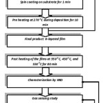
Zinc acetate dihydrate, iso-propanol, ethanol amine, analytical grade reagents (Sigma Aldrich) are used as the precursors for the sol preparation. Initially, zinc acetate dihydrate (3.10 gm) is dissolved in iso-propanol (15 ml). Ethanol amine (0.86 ml) is then added to the zinc acetate solution with ethanol amine to zinc acetate molar ratio 1:1. The mixture is continuously stirred at 600C for 60 minutes.40-43 The sol, thus obtained, is then aged for 24 hrs for gelation to occur. ZnO thick films are deposited on precleaned glass substrate by sol gel spin coating technique. Cleaned glass substrates are fixed on the spin coater and are spun at 2500 rpm for about 1 minute while aged gel is dropped onto a glass substrate. The obtained single layer film is then heat treated in air oven at 270OC for about 10 minutes for the decomposition of the precursor components & formation of metal-oxides. Thus, six layered film is deposited by spin coating, followed by baking at 270OC after deposition of each layer, resulting in a thick film. These six layered films are annealed at a temperature of 350OC and are used as sensors for further studies. Figure 1 gives flowchart of sol gel spin coating process of ZnO thick films.
Figure 1: Flow chart of methodology used for preparation of sol gel deposited ZnO thick films
Film Modification
The ZnO films, mounted on a ladder in high voltage irradiation chamber, are modified by exposing them to heavy ion beam with a fixed dose of 3×10¹¹ ions / cm2. Films of about 1 cm2 area are irradiated with 100 MeV Ag7+ ions using 15UD Pelletron tandem accelerator installed at Inter University Accelerator Centre, New Delhi. Beam current is maintained around 1 nano ampere. Ion beam, focused to a spot of 1 mm diameter, is then scanned over 1 cm × 1 cm area using a magnetic scanner. Through out the experiment the vacuum of the order of 10-6 torr is maintained. In our experiment, high energy is selected to have the range of the ions upto few microns in the material so that no ions are implanted in the film and there will be only defects due to the irradiation. The SRIM analysis of the Ag7+ with 100 MeV ions bombarded on the ZnO thick film has shown that electronic energy losses dominate the nuclear energy losses. Using SRIM, the projected range of the ion in ZnO is determined and it is found to be approximately 50 µm.
Characterization by X-ray Diffraction
The pristine and irradiated sensors are subjected to XRD analysis. The crystalline phase of ZnO thin films is identified using Rigaku make X-ray powder diffractometer (Miniflex). The samples are irradiated with monochromatic CuKα radiation having a wavelength of 1.542 A0and the XRD patterns are recorded over a 2θ range of 300 to 700.
Gas Sensing Study
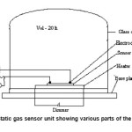
The pristine and irradiated sensors are tested for sensing response to carbon dioxide. The CO2 gas sensing study on pristine and ion beam irradiated ZnO films is carried out using static gas characterization system as shown in figure 2. The fabricated sensor is placed in the test chamber of known volume. For the measurement of gas response, a load resistor is connected in series with a gas sensor. The circuit voltage is set at 30 V, and the output voltage measured across load resistor. The working temperature of a sensor is varied through varying the heating voltage of the heater. The sensor film is initially heated from RT to 400 OC and voltage drop (Vr) across resistor (Rr) in air atmosphere is measured at a selected interval of temperature. A known volume of the CO2 gas is injected inside the system to establish required gas concentration using a doctor’s syringe followed by measurement of voltage drop across resistor (Rr) in gas environment as a function of temperature. The electrical resistance of the film in air (Ra) and in the presence of CO2 gas (Rg) is determined by using the formula42
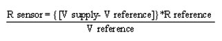
Figure 2: Static gas sensor unit showing various parts of the system
V Reference
The change in resistance of the ZnO thick film, when exposed to a test gas, is determined to evaluate the gas response or sensitivity factor and the percentage sensitivity factor is calculated by using the following formula [42].
SF = [Rg – Ra]/Ra*100 = ( Δ R/ Ra*100)
A graph of gas response as a function of temperature with a fixed gas concentration is plotted to determine the operating temperature of the sensor film. The operating temperature is defined as the temperature at which the sensor film has maximum gas response SF (%). The gas uptake capacity of the sensor film is optimized by exposing the virgin as well as irradiated films to a gas of variable concentration.
Results and Discussion
XRD Analysis
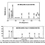
Figure 3(A-B) represents the X-ray diffraction profiles ZnO thick films before and after SHI irradiation at a fixed fluence of 100 MeV Ag7+ ions. The XRD analysis is carried out using the JCPDS card (36-1451) for ZnO by search/match method. Both the XRD patterns exhibit all the peaks corresponding to the standard wurtzite hexagonal structure. It has been observed that [101] reflections corresponding to 2θ = 36.17° are of maximum intensity for both the film samples. This indicates that virgin as well as SHI modified ZnO films have strong orientation in the direction of [101] plane. All these peaks are also found to be matching with standard data and literature.38 From the XRD profile of modified ZnO film it can be revealed that there is increase in intensity and sharpness. It can be concluded that irradiation leads to increase in crystallinity of the ZnO film. The crystallite sizes, estimated for (101) peaks of pure and modified XRD patterns using Scherrer’s formula, are found to be 35 nm and 20 nm respectively. It is observed that even after irradiation with 100 MeV Ag7+ ions, the modified ZnO film shows the crystalline phase. Thus it can be concluded that the influence of ion irradiation do not lead to amorphisation in case of ZnO. This result is in consistence with literature.38
Figure 3 : XRD profiles of the ZnO sensor films deposited on glass substrate via sol gel spin coating technique and sintered at 350 °C; A) Pristine ZnO sensor, B) Modified ZnO sensor
Analysis of Gas Sensing Study
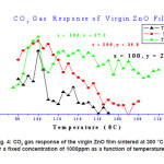
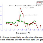
Figure 4 represents a typical variation of sensitivity factor for a pristine sample sintered at 3500C as a function of temperature for 1000 ppm of CO2. It is observed that sensitivity factor shows drastic change in the temperature range 900C to 1100C. It reaches a maximum sensitivity value of 37.3 at 1000C & then decreases with further increase in temperature. This behavior indicates that optimum operating temperature of a six layered pure ZnO film is 1000C.
Figure 4: CO2 gas response of the virgin ZnO film sintered at 300 °C for a fixed concentration of 1000ppm as a function of temperature
Figure 5 depicts the temperature dependence of gas response of modified ZnO thick film. Similar kind of behavior is shown by the modified ZnO film wherein the sensitivity factor initially increases with temperature, shows a maxima at 1500c & then decreases further at higher temperatures. The modified sensor displays the maximum highest sensitivity of the order of 73.8 at 150°C for 1000ppm CO2 gas. However, it is worth to note that in both the films after every cycle decrease in response is observed.
Figure 5: Change in sensitivity as a function of temperature in SHI irradiated ZnO film for 1000 ppm CO2 gas
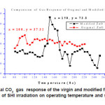
Figure 6 shows the effect of SHI irradiation on operating temperature and sensitivity. It can be concluded that irradiation effect leads to shift in operating temperature and enhancement in sensitivity factor compared to that for pure sample.
Figure 6: Typical CO2 gas response of the virgin and modified films showing the effect of SHI irradiation on operating temperature and sensitivity
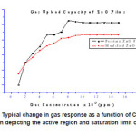
The sensor response in the range 1000 to 14000 ppm, for pristine and modified ZnO films when operated at 100°c and 150°c, is presented in figure 7. It can be concluded that gas uptake capacity is not affected by the SHI irradiation because both films show saturation at 8000 ppm.
Figure 7: Typical change in gas response as a function of CO2 gas concentration depicting the active region and saturation limit of the sensor
Further increase in CO2 gas concentration does not show any significant change. This reveals that the active region of the sensors is up to 8000 ppm.
The electronic behavior of the semiconductor material plays a major role in the sensor applications. In semiconducting oxide based gas sensor like ZnO, the sensing mechanism is considered as the adsorption phenomenon. Upon the adsorption of gases the electrical conductance of semiconductor changes and can be correlated to the gas present in the ambient atmosphere.
The adsorption process can be grouped as physiosorption, chemisorption and ionosorption. Ionosorption process, dominant in metal oxide semiconductors, involves capture of holes or of electrons or give up electrons.
The surface of ZnO is ionic in nature. Its surface metal ion can capture electron and the surface oxygen ions give up an electron. At room temperature donor levels near to the conduction band are completely ionized. But below conduction band, donor levels are not completely ionized. Thus the density of donor level in conduction band can be increased with increasing temperature or by exposing to gases.
The gas sensing mechanism is either by adsorption of atmosphere oxygen of the surface and/ or by direct reaction of the lattice oxygen or interstitial oxygen with the test gases.
When the atmospheric oxygen adsorbs on the surface, it extracts an electron from the conduction band, and formation of oxides or peroxides takes place. They are mainly responsible for the detection of the test gases.
O2 + e– → 2O–
This adsorbed oxygen ion decreases the electrical conductance of the semiconductor.
Whereas the reducing gases R, present in the ambient, react with the oxygen ions by trapping the electrons and liberating into the conduction bond. This leads to the increase in conductance in semiconductor.
R + O – → RO + e–
This reaction of the conductance of the semiconductor due to this reaction can be accelerated by the presence of suitable catalyst or doping.
Thus the gaseous molecules split into ions and spread over the semiconductor surface and reacts with the lattice oxygen ion. If sensor material is with sufficient activation energy then the ionized reducing gas itself get spread over the surface of the semiconductor. In addition to this defect structure consisting of oxygen of vacancies and interstitial oxygen ions also contribute to this mechanism. In such situation the reactions can be written in terms of krogervink notations.
O0 → V0++ + O1– –
R + Oi– – → RO + 2e–
Where,
O0 = The lattice oxygen.
V0 ++ = The oxygen vacancy in the lattice.
O — = The interstitial oxygen
Reaction of the reducing gas with the interstitial oxygen provides two electrons to the sensor material and there by the conductance increases.
Thus, ZnO sensor works on the adsorption of oxygen on the available surface site and the reaction between adsorbed oxygen and the test gas (CO2) is the cause of change in resistance of the sensor material. The decrease in sensitivity factor (R) at higher temperature may be due to desorption of pre-adsorbed oxygen ions from the surface of the sensor.
The ZnO thick films are prepared successfully using sol gel spin coating technique. The ZnO films are modified by the use of 100 MeV Ag 7+ ion beam. Both, the virgin and irradiated ZnO films possess hexagonal wurtzite structure with c =5.271Ao and a = 3.285Ao. The crystallite size, estimated using Debye – Scherer formula, for as deposited ZnO films and modified film are 35 nm and 20 nm respectively. Irradiation leads to increase in crystallinity and reduction in average crystal size for modified ZnO films. The optimum operating temperatures for pure & modified ZnO films are found to be 1000c & 150 0c respectively. The change in operating temperature is due to swift heavy ion irradiation effect. Sensitivity factor of sol gel prepared ZnO film towards CO2 has been improved by modifying it with Ag+7 irradiation. There is no effect of SHI irradiation on saturation in terms of concentration. Modified as well as unmodified ZnO have the working range of 8000ppm.
Acknowledgements
Authors would like to thank Hon’ble Vice-Chancellor Dr. S.B. Nimse, SRTM University, Nanded for his constant encouragement. Thanks to Inter University Accelerator Center for providing Ion Beam facility. Thanks to Prof. D.K. Avasthi, IUAC for his valuable guidance.
References
- Dong H.K., Ji Y.Y., Hee C.P., Kwang H.K,Sensors Actuators B 62: 61-66 (2000).
CrossRef
- Herran, J., Mandayo, G.G., Castano, E, Thin Solid Films 517: 6192-6197 (2009).
CrossRef
- Adhikari B., Majumdar S., Prog. Polym. Sci.,29: 699-766 (2004).
CrossRef
- Xiaowen Xu, Jing Wang, Yingcai Long,Sensors, 6: 1751-1764 (2006).
CrossRef
- Chapelle A., Oudrhiri-Hassani F., Presmanes L, Barnabé Ph.. Tailhades A., Applied Surface Science, 256: 4715-4719 (2010).
CrossRef
- Suchea M., Christoulakis S., Moschovis K.,Katsarakis N., Kiriakidis G., Thin Solid Films 515: 551-554 (2006).
CrossRef
- More P.S., Khollam Y.B, Deshpande S.B.,Date S.K., Karekar R.N., Aiyer A.C., Material letter, 57: 2177-2184 (2003).
CrossRef
- More P.S., Khollam Y.B, Deshpande S.B.,Date S.K., Karekar R.N., Aiyer A.C, Material letter, 58: 205-210, (2003).
CrossRef
- Bhole M. P., Patil D. S., Photoelectronics and advanced materials-rapid communications,1(12): 672 -676 (2007).
- Dutta S., Jackson H.E., Boyd J.T., Hickernell F.S. and Davis R.L., Appl. Phys. Lett., 39:206-208 (1981).
CrossRef
- Sahay P.P., Tewari S., Nath R.K., Cryst. Res.Technol., 42(7): 723-729 (2007).
CrossRef
- Patil D. R., Patil L. A. and Amalnerkar D. P.,Bull. Mater. Sci., 30(6): 553-559 (2007).
CrossRef
- Joseph B., Gopchandran K.G., Manoj P.K.,Koshy P., Vaidyan V.K., Bull. Mater. Sci., 22:921-926 (1999).
CrossRef
- Chou. S. M., Teoh L. G., Lai W. H., Su Y. H.and Hon M. H., Sensors, 6(10): 1420-1427(2006)
- Trivikrama Rao S. G. and Tarakarama Rao D., Sen. Actu. B, 55: 166–169 (1999).
CrossRef
- References and further reading may be available for this article. To view referencesand further reading you must purchase this article. Bie L.J., Yan X.N., Yin J., Duan Y.Q.and Yuan Z.H., Sensors and Actuators B:Chemical, 126 (2): 604-608 (2007).
- Lupan O., Ursaki G., Chai, L., Chow G.,Emelchenko A, Tiginyanu I.M, GruzintsevA.N. and Redkin A.N., Sensors and Actuators B: Chemical, 144(1): 56-66 (2010).
CrossRef
- Mitra P., Mukhopadhyay A.K., Bull. Pol.Ac.:Tech. 55(3): 281-285 (2007)
- Shishiyanu S. T, Shishiyanu T.S., Lupan O.I,Sensors and Actuators B, 107: 379-386(2005)
CrossRef
- Roy S. and Basu S., Bull. Mater. Sci., 25(6):513–515 (2002)
CrossRef
- Lupan O., Shishiyanu S., Chow L.,Shishiyanu T., Thin Solid Films, 516: 3338–3345(2008)
CrossRef
- Zhang Y., Xu J.,, Xiang Q., Li H., Pan Q. and Xu P., J. Phys. Chem. C, 113(9): 3433 (2009)
CrossRef
- Zhang J., Wang S., Xu M., Wang Y., Zhu B.,Zhang S., Huang W. and Wu S., Cryst.Growth Des., 9(8): 3532-3537 (2009).
CrossRef
- References and further reading may be available for this article. To view references and further reading you must purchase thisarticle.Lim H.J., Lee D.Y. and Oh Y.J., Sensors and Actuators A: Physical, 125(2):405-410 (2006)
- Suchea M., Christoulakis S., Moschovis K.,Katsarakis N., Kiriakidis G., Thin Solid Films,515: 551-554 (2006)
CrossRef
- Anderson T , Ren F., Pearton S., Sam Kang B., Wang H.T., Chang C. Y. and Lin J., Sensors 9: 4669-4694 (2009)
CrossRef
- 4760abstractLu C.Y. Chang S.P., Chang S.J. , IEEE International Conference on Electron Devices and Solid-State Circuits,(EDSSC), 8-10 Dec (2008)
- Zhang N. Y., Ke L. Q. , Zhu Z. Q., Wan Q, Journal of Applied Physics, 103: 104305-6 (2008)
CrossRef
- Lupana O., Chowa L., Chaid G., Sensors and Actuators B 141: 511-517 (2009)
CrossRef
- Liao L. , Lu H. , Shuai M. , Li J. , Liu Y. , Liu C., Shen Z., Nanotechnology, 19(17): 175501 (2008).
CrossRef
- Samasekara P. Yapa N.U.S., Kumara N.T.R.N., Parera M.V.K., Bull. Mater. Sci., 30(2): 113-116 (2007).
- Paraguay D F. and Miki-Yoshida M., Superficies y Vacío 9: 245-247 (1999).
- Paraguay D F., Miki-Yoshida, Morales J.,Estrada L.W., Thin Solid Films 373: 137-140(2000).
- Chadwick A.V., Harsch A., Russell N.V., Tse K. F., Whitham A. R., Wilson A., Radiation Effects and Defects in Solids: Incorporating Plasma Science and Plasma Technology, 137: 51-55 (1995).
- Avasthi, D.K., Curr. Sci 78: 1297-1302 (2000).
- Avasthi D.K., Ghosh S., Srivastava S.K., Assmann W., Nucl Instrum. Methods B, 219-220 (2004).
- Liao L., Lu H. B., Li J. C., Liu C., Fu D. J., and. Liu Y. L, Appl. Phys. Lett., 91: 173110 (2007).
CrossRef
- Singh R. C., Singh M.P., Singh O., Chandi P.S. and Kumar R., Appl Phys A: Materials Science and Processing, 98: 161-166 (2010).
CrossRef
- Watanabe K., Matsumoto K., Ohgaki T., Sakaguchi I., Ohashi N., Hishita S., andHaneda H., Journal of the Ceramic Society of Japan,118(1375): 193-196 (2010).
CrossRef
- Habibi M. H. and Sardashti M. K.,J.Iran.Chem.Soc., 5(4): 603-609 (2008).
CrossRef
- G. Srinivasan, and J. Kumar, Cryst. Res.Technol. 41(9): 893-896 (2006).
CrossRef
- Ilican S., Caglar Y., Caglar M., J. of Optoelectronics and Advanced Materials,10(10): 2578-2583 (2008).
- Natsume Y., and Sakata H., Thin solid Films,372: 30-36 (2000).
CrossRef
- CrossRef

This work is licensed under a Creative Commons Attribution 4.0 International License.