K. Yadaiah1*, J.Krishnaiah1, Vasudeva Reddy2 and M. Nagabushanam2
¹Sri Venkateswara College (U.G. and P.G.), Suryapet - 508 213 (India).
²Department of Physics, Osmania University, Hyderabad - 500 007 (India).
DOI : http://dx.doi.org/10.13005/msri/090104
Article Publishing History
Article Received on : 10 Jun 2012
Article Accepted on : 28 Jul 2012
Article Published :
Plagiarism Check: Yes
Article Metrics
ABSTRACT:
The Polycrystalline (CdSe)1-x(ZnS)x semiconductor powder with 0<=x<=1 was prepared by controlled co-precipitation method. Pellets made out of the powder, sintered at 800o C in nitrogen atmosphere was used for studies. Electrical conductivity of these samples increased with increasing the temperature from 77-300o K. At a given temperature an increase in conductivity with the increase in composition was observed in samples with x = 0.2 to 0.4 where as decrease in conductivity with the increase in composition occurs in samples with x = 0.7 to 1. For all samples, activation energies were calculated from the linear portions of log s vs 1000/T and the values range between 0.021 eV to 0.042 eV measurements of all samples are found to be negative, indicating n-type conduction in temperature region 77-300oK.From TEP and conductivity studies, carrier concentration and their mobilities were deduced and all the results were reported and suitable reasons were attributed for each observation made.
KEYWORDS:
Electrical Conductivity; Thermo Electric Power; Charge Carrier Concentration; Mobility
Copy the following to cite this article:
Yadaiah K, Krishnaiah J, Reddy V, Nagabushanam M. Electrical Conductivity, TEP and Mobility of (CdSe)1-x(ZnS)x Mixed Semiconductors. Mat.Sci.Res.India;9(1)
|
Copy the following to cite this URL:
Yadaiah K, Krishnaiah J, Reddy V, Nagabushanam M. Electrical Conductivity, TEP and Mobility of (CdSe)1-x(ZnS)x Mixed Semiconductors. Mat.Sci.Res.India;9(1). Available from: http://www.materialsciencejournal.org/?p=1150
|
Introduction
Mixed semiconducting materials, especially the Cadmium chalcogenides, form a technically important class of materials because of their wide spread utility in a variety of opto-electronic devices. The main reason for this utility was that their optical energy gaps could be tailored to match with a sensitive region of the visible spectrum and they possess effectively high photosensitivity over a wide range of the photon energies. During the last decade, a variety of binary semiconductors formed out of II and VI group of elements of the periodic table have been studied extensively due to their potential use as Photoconductive devices and Solar cells. CdSe is one of the members of the II-VI family having a suitable band-gap to match the maximum solar spectrum and high photosensitivity. CdSe, with some additives in it, forms an important class of semiconductor materials with which one can prepare low cost devices. One of the modern approaches in the search for effective thermoelectric materials consists of creation of new ternary and quaternary chalcogenides with complicated crystal structure, narrow band-gaps and complex electronic structures near the Fermi energy. They also play an important role in device areas such as Solar energy conversion devices, and diode elements etc. Therefore the study of transport properties of chalcogenides and their mixed crystals in bulk, as well as in thin film form becomes an essential. Particularly, quaternary crystals like (CdSe)1-x(ZnS)x will be more useful in electronic industry due to their interesting electronic properties with the variation of temperature.
A considerable amount of both theoretical and experimental work has been aimed to provide a quantitative description of the relationship between the current and material concentration and the fabricating parameters. (CdSe)1-x(ZnS)x solid solution is an especially interesting quaternary system for the study of the role of thin film in framing the bulk properties of polycrystalline (CdSe)1- x(ZnS)x with hexagonal and cubic structure. It has been found that the conductivity of (CdSe)1-x(ZnS)x
quaternary thin films are useful for its device application as infrared detector measured as a function of film thickness, ZnS content and temperature.
M.A. Afifi and others1 have prepared Znx Cd1-xS thin films over the entire range of x, the electrical resistivity of Znx Cd1-xS thin films was measured as a function of the film thickness, the ZnS content and the film temperature. The thermal activation energy for electrical conduction increases with the increase of ZnS content. The film thickness was controlled using a thickness monitor and then measured applying Tolansky’s method2. Research on chalcogenide semiconductors still continues
because of their possible technological applications and transport properties.
L.P Deshmuhk and K. Sharma and B. Singh3-6 have reported their results on TEP behavior of (CdS)x(PbS)1-x thin films as a function of different deposition parameters. Their results have shown that the TEP increases with increasing substrate temperature and film thickness.
J.A. Rodreguez and G. Gordillo7 have reported the electrical properties of ZnCdS films and are observed that they are strongly influenced by the Zn content on the evaporation parameters. Increase of the Zn concentration in ZnCdS films leads to decrease of both, the density, and mobility of free carriers and resistivity of the films. The result showed that the conductivity of ZnCdS films, in the high temperature range is dominated by transport of electrons in the conduction band while in the range of lower temperatures, the conductivity is dominated by transport of electrons across the impurity levels. L.P. Deshmukh8 carried out TEP measurements on (CdS)x(PbS)1-x films and reported that TEP decreases with the increase in the parameter x from 0 to 0.5 and increases for further increase in the value of x. From the literature, it is found that much work has been done on transport properties such as (DC electrical conductivity, TEP, mobility and charge carrier concentration) in thin
films of semiconductor compounds grown in different methods. But no systematic work has been done on bulk form of ternary and quaternary semiconductors of the type (CdSe)1-x(ZnS)x grown by co-precipitation method. Therefore, in order to understand the conduction mechanism of transport properties in bulk (CdSe)1-x(ZnS)x, the present studies are undertaken at different temperatures (77oK-300oK). Also from the literature it is clear that the thermoelectric properties of material in thin film and bulk forms of large number of materials like metals, semiconductors have been studied but the study of TEP on ternary and quaternary semiconductors in the bulk form is limited.The results obtained on electrical conductivity, thermoelectric power of bulk (CdSe)1- x(ZnS)x (x = 0-1) chalcogenide polycrystalline semiconductors are presented at low and high temperature regions and discussed. The results are explained based on their related properties in semiconductors.
Experimental
Mixed (CdSe)1-x(ZnS)x powder was prepared by controlled co-precipitation method9. The dried precipitate was transferred into a clean and dry quartz boat and was kept in a quartz tube of diameter 3 cm and 1 m length, which was arranged, in a high temperature tubular furnace (0°-1000°C). Both the ends of quartz tube were provided with two metal caps to pass inert gas through the tube. The precipitate was heated in a tubular furnace under Nitrogen atmosphere for 2 hours at 300°C. Then the furnace was cooled to room temperature slowly. The precipitate was grind to form a fine powder and the process is repeated in order to obtain the uniform particle size. The powder is made into pellets under pressure by using a punch die of 1.5 cm diameter. The hydraulic pressure applied for pellet formation was 10 tonnes per square cm and the duration of time was about 10 minutes. Necessary amount of powder was taken every time to obtain the pellets of about 1 mm thickness, the pellets were heated at 800°C for 2 hours under the Nitrogen atmosphere. The pressure of the gas was maintained uniform throughout the heating process and the furnace was cooled very slowly (1°C/minute) to room temperature.
A four-probe technique was used to perform the electrical conductivity studies. High pure Indium (99.99%) was used for electrical contacts. The contacts were made at 300°C temperature under inert atmosphere. Kiethley nanovoltmeter model 182 was used to measure potential drop across the sample and a Kiethley multimeter model 2000 was used to measure the output of the temperature sensor (copper-constantan thermo couple). A Kiethley constant current source model No. 224 was used to pass the current through the sample.
Results and Discussion
Electrical conductivity
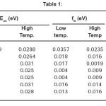
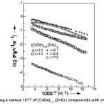
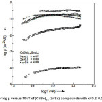
The electrical conductivity (s) of (CdSe)1- x(ZnS)x polycrystalline samples has been measured in the temperature range 77–300°K. A typical variation of log s vs 1000/T of (CdSe)1-x(ZnS)x samples with x = 0.2 ≤ × ≤ 1 are shown in the Fig. 1. It is understood, in general from the graphs that the electrical conductivity increased with increasing temperature. The temperature dependence of σ with temperature can be expressed by the usual Arrheneous equation as where Eaσ is the conductivity activation energy. At a given temperature an increase in conductivity with the increase in composition was observed in samples with x = 0.2 to 0.4. This may be due to the decrease in band gap and an increase in disorderness in the structure of the samples with the introduction of ZnS into CdSe lattice. Whereas, decrease in conductivity with the increase in composition occurs in samples with x = 0.7 to x = 1. This may be due to the increase in band gap and decrease in disorderness in the structure of the sample with the introduction of ZnS into the lattice of CdSe. For all the samples activation energies have been calculated from the linear portions of log s vs 1000/T, shown in Fig. 1, and are listed in Table – 1.
Table 1
It is observed from the Table that the conductivity activation energy at lower and higher temperature zones decreases with increase in concentration of ZnS from x = 0.2 to 0.7 and it increases as x varies from x = 0.8 to 1.0. This result may be correlated with the variation in resistivity and conductivity10, 11
TEP measurements
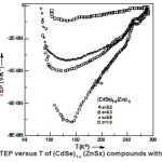
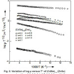
The thermo emf of (CdSe)1-x(ZnS)x polycrystalline semiconducting samples with x = 0 – 1 was measured as a function of temperature in the temperature region 77 – 300° K. The polarity of the thermally generated voltage at the hot end of all samples was positive, indicating that the samples are of the n-type. Fig. 2 shows the variation of TEP with temperature for samples of (CdSe)1- x(ZnS)x with different values of x = 0.2, 0.3, 0.7, 0.8, and 1.0. In general, the Fig 2 shows that the thermoelectric power decreases with increase in temperature in the temperature region. (77-150oK), attains a minimum and increases in the higher temperature region 150 – 300° K..
However the value of TEP remains negative at all temperatures, which indicates the ntype nature of the sample, does not change. The decrease in TEP with the increase in temperature (till it attains minimum) indicates an increase in the electron concentration and later this increase is modified with the positively charged carriers produced which nullifies the effect of negative charge carriers to some extent and still remain as electron dominant material causing an increase in TEP with the temperature (after the minimum point). Since TEP has a negative sign over the entire temperature range of investigation, the samples possess electrons as majority carriers. i.e.
Figure 1: Variation of log s versus 10³/T of (CdSe)1-x (ZnSx) compounds with x=0.2, 0.3,0.7,0.8 & 1.0
Figure 2: Variation of TEP versus T of (CdSe)1-x (ZnSx) compounds with x=0.2, 0.3, 0.8 & 1.0
(CdSe)1-x(ZnS)x crystals exhibit n-type conductivity in the temperature region (77 – 300 °K). It is observed from the Fig.2 that the temperature dependence of TEP is approximately non-linear (before and after obtaining minimum value) and supports the power law dependence of temperature. The TEP is proportional to the nth power of the absolute temperature. For such cases the dependence of TEP on temperature is weaker and follows the exponential variation12.
Figure 3: Variation of log n versus 10³/T of (CdSe)1-x (ZnSx) compounds with x=0.2 and 0.9
Figure 4: Variation of log μ versus 10³/T of (CdSe)1-x (ZnSx) compounds with x=0.2, 0.3, 0.4, 0.7, 0.8, 0.9
Figure 5: Variation of log μ versus T½ of (CdSe)1-x (ZnSx) compounds with x=0.2, 0.3, 0.4, 0.7, 0.8, 0.9 and 0.10
Where r + 5/2 = A, a thermoelectric factor which depends on various scattering mechanisms m* is the effective mass and n is the charge carrier concentration. Solving the above equation with appropriate values of A and m* we can write an important relation for application13 i.e.,
Log n = 3/2 (log T) – 0.005 (TEP) + 15.719 …(3)
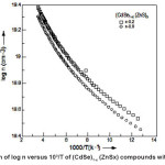
Charge Carrier Concentration (n) The TEP is empirically related to the carrier concentration n given by the Equation 3. The charge carrier concentration for all (CdSe)1-x(ZnS)x samples was calculated by using the Equation 3. The Fig. 3 shows a typical variation of log n with inverse temperature for two samples of (CdSe)1-x(ZnS)x with x = 0.2 and x = 0.9. In general it is observed from this figure that
- the carrier concentration is of the order of 1019 cm-3 and charge carrier concentration n increases with the temperature in all the samples.
- there is not much appreciable change in n with the composition (x). From these curves the activation energies of all the samples are calculated in lower and higher temperature regions and are given in Table-1. From this Table it is also observed that in each sample Ean of higher temperature region is more than that of lower temperature region.
Mobility of Charge Carriers
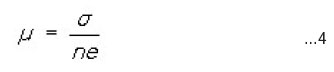
If the conduction of (CdSe)1-x(ZnS)x semiconductors is assumed to be predominantly due to only one type of charge carries i.e. electrons/ holes the mobility of charge carriers (μ) can be calculate by the equation.
The values of charge carrier mobilities were calculated for all (CdSe)1-x(ZnS)x samples using the experimental values of electrical conductivity (s) and carrier concentration n obtained from TEP data using the equation 3. The temperature variation of mobility (logm vs LogT) of (CdSe)1-x(ZnS)x polycrystalline samples with x = 0.2 – 1.0 is shown in Fig. 4. One can note that the charge carrier concentration is a weak function of composition (x) but it varies with temperature as shown in Fig. 3. The interesting result in all the samples is that the mobility increases significantly with the temperature as well as with the composition in the observed temperature region (77 – 300° K). It is worth noting that R. Venugopal and B.K. Reddy14 have reported similar results in ZnSe0.5 CdS0.5 alloy films and they attributed their results to the complicated behaviour of the mobility against temperature. The carrier mobilites in films formed at higher temperatures are comparatively higher. This is due to an increase in crystallinity and also due to an improvement in the stoichiometry of the films formed at higher temperature. Further, the high temperature mobilities are higher than the low temperature mobilities in films formed at both the substrate temperatures. Kowk and Siu15 reported similar increase in mobility with temperature in CdS films.
The different scattering mechanisms that control the Hall mobility in II-VI thin films are bulk scattering (B), space charge region scatterings in the grains (g), intergrain boundary (gb) and Schrieffer’s scatterings. The bulk scattering in II-IV semiconductor includes piezoelectric, ionized impurity and phonon scatterings. Among all these, grain boundary scattering and ion impurity scatterings have the characteristic feature of increasing mobility with temperature. However, the degree of increase of mobility with temperature in the present study resembled more the grain boundary scattering similar to CdS films. Waxman et al.,16, give the expression for grain boundary controlled mobility.
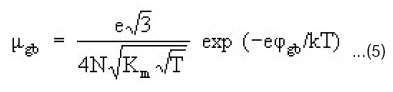
where e is the electron charge, N, the number of crystallites, k, the Boltzmann constant, T the absolute temperature, and φgb, the intercrystalline barrier height (Grain boundary potential). In the present study, we noticed that the mobility increases with the increase in composition (x) from (0.2 – 0.4) and decreases later with further
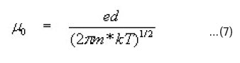
increase in x till 1.0. Thus the increase in mobility with the temperature suggests the possibility of scattering mechanism associated with the intergrain barrier height as proposed by Petritz17. According to him the temperature dependent grain boundary mobility is calculated with the grain boundary potential as
μ = μ0 T-1/2 exp (-φB/kT) ….(6)
Where fB is the height of the potential barrier at the grain boundary, which can be determined from the slope of the variation of log (mT1/2) versus 1000/T (Fig. 5) and μ0 is the preexponential factor, which on the assumption that the current over the barrier flows by thermo-ionic emission depends on the grain size (d) and the effective mass of electron (m*) as18.
The height of the potential barrier at the grain boundaries in all samples were calculated from these graphs and are shown in Table.3.1. From the observed values of the activation energies of electrical conductivity (Eaσ) and electron density (Ean) (calculated from log n versus 1000/T especially at low temperature) and potential barrier height at the grain boundary (φB), the relation.
Eas = Ean + φB …(8)
holds good. This is expected from the inter relationship between the electrical conductivity, carrier density and mobility17, 18. A similar result was also observed by R.N. Mullik et al.19 in polycrystalline lead selenide thin films. Most commonly the films contain large number of grain boundaries and in (CdSe)1-x(ZnS)x polycrystalline samples prepared by sintering technique, also one can expect large number of grain boundaries and a similar type of relation between Eas, Ean and fB. It is seen that the carrier concentration though depends on temperature it does not depend much on the composition, whereas mobility depends on both of them. Hence it may be presumed that the grain boundaries are not acting as charge carrier-trapping agents but are modifying the mobilities on account of their low boundary potential.
Conclusion
- Electrical conductivity and thermoelectric power studies of polycrystalline (CdSe)1- x(ZnS)x samples have been conducted between the temperature ranges 77 – 300° K. From these studies, charge carrier concentration and their mobilities at different temperatures have been deduced.
- The dependence of electrical conductivity, thermoelectric power, charge carrier concentration and mobility on temperature and composition are explained in terms of grain boundary scattering mechanisms.
- In polycrystalline (CdSe)1-x(ZnS)x semiconductors with x = 0.2 – 1.0, the electrical conductivity is observed to increase with increasing temperature and in each composition, it showed three different linear regions in different temperature ranges. The conductivity activation energies are determined from these linear regions and the values range between 0.021 eV to 0.042 eV.
- The thermoelectric power measurements of (CdSe)1-x(ZnS)x are found to be negative, indicating n-type conduction in temperature region 77 – 300° K and also show that the temperature dependence of TEP in the lower and higher temperature range is non-linear.
- (CdSe)1-x(ZnS)x compounds have shown typical variation of charge carrier concentration n with temperature i.e. n increases with the temperature, but no appreciable change in ‘n’ with the composition x.
- The temperature variation of carrier mobility in (CdSe)1-x(ZnS)x with x = 0.2 – 1.0 showed that the mobility increases significantly with the temperature as well as with the composition from x = 0.2 – 0.4 and later it decreases from x = 0.7 – 1.0. The observed increase in mobility with temperature may be due to charge carrier scattering associated with the intergrain barrier.
References
- M.A. Afifi et al., Indian J. of Pure and Appl. Physics 24: 550 (1986).
- S.Tolanky, Multiple beam Interferometry of surfaces and films (Oxford University Press, London) 147 (1948).
- L.P.Deshmukh. et al., Bull. Mater. Sci. 17(5): 455 (1994).
CrossRef
- L.P.Deshmukh. et al., Indian J. Pure and Appl. Phy. 34: 893 (1996).
- R.N. Mullik, C.B. Rotti, L.P.Deshmukh. Indian J. Appl. Phy. 34: 903 (1996).
- Arun K. Sharma and B. Singh, Indian J. Pure and Appl. Phy. 23: 84 (1985).
- J.A. Rodriguez, and G. Gordillo, Solar energy materials. 19: 421 (1989).
CrossRef
- L.P.Deshmukh. et al., Bull, Mater, Sci. 17(5)455 (1994).
CrossRef
- K.Yadaiah, Abdul Nayeem, M.Somi Reddy and M.Nagabhooshanam, International J. Modern Physics B, Vol. 16, 19(2002) 2885.
CrossRef
- A. Rohatgi, lr. Viverits and l.H.J. Slack Aam cemma Soc., 57: 278 (1974).
- L.P. Deshmukh, C.B. Roti, K.M.G. and P.P. Hankare, Indian J. of Pure and Appl. Physics 34: 893 (1996).
- I.Ravich Yu, B.A. Efimova and Smirnov, in method of semiconductor investigations : Application to lead chalcogenides PbTe, PbSe, PbS (Izd NoUka, Moscow), (1968).
- R.R. Heikes and R.W. Ure Jr. Thermoelectricity Science & Engineering (Interscience, New York) (1961) Chapter 3.
- R. Venugopal, R.P. Vijayalakshmi, D.R. Reddy, and B.K. Reddy, Materials Research Bulletin, 30(11): 1431 (1995).
CrossRef
- H.L. Kowk, and W.C. Siu, Thin Solid Films. 61: 249 (1979).
CrossRef
- A. Waxman, V.F. Henrich, F.V. Shallcross,N. Borkan, and P.V. Wiemer, J. Appl. Phys. 36: 168 (1965).
CrossRef
- R.L. Petritz, Phy. Rev. 104: 1508 (1956).
CrossRef
- G. Micocci, A. Jepore, R. Rella, and P. Sicihano, Phys. Status Solidi, 148: 431 (1995).
CrossRef
- R.N. Mullik, C.B. Rotti, B.M. More, D.S. Sutrave, G.S. Shahane, K.M. Garadkar, L.P. Deshmukh and P.P. Hankare. Indian. J. Pure and Appl. Phys. 34: 903 (1996).

This work is licensed under a Creative Commons Attribution 4.0 International License.