The supply of clean energy for our society is a central challenge to maintain our standard of living. It is important to change from fossil fuels to renewable energy sources for two main reasons: Firstly, the natural resources of gas and oil are limited and will run out. Secondly and more importantly, a continued dependence on fossil fuels would increase an already alarming rate of CO2 emission. Additionally, other environmental problems caused by the mining of these resources may increase because the remaining resources will be in places which are more difficult to reach. Solar cells are promising candidates for CO2 emission free energy supply. Hence, developing environmentally friendly, renewable energy is one of the challenges to society in the 21st century. One of the renewable energy technologies is photovoltaics (PV), the technology that directly converts daylight into electricity. PV is one of the fastest growing of all the renewable energy technologies; in fact, it is one of the fastest growing industries at present.1 Solar cells are designed to convert available light into electrical energy. They do this without the use of either chemical reactions or moving parts. Solar cell manufacturing based on the technology of crystalline, silicon devices is growing by approximately 40% per year and this growth rate is increasing.1 This has been realized mainly by special market implementation programs and other government grants to encourage a substantial use of the current PV technologies based on silicon. The silicon is treated or ‘‘doped’’ in order to create charge carriers, so that when light strikes it electrons are released, leading to generation of electric current. The active materials used for the fabrication of solar cells are mainly inorganic materials, such as silicon (Si), gallium- arsenide (GaAs), cadmium-telluride (CdTe), and cadmium-indium-selenide (CIS). The power conversion efficiency for these solar cells varies from 8 to 29%. The current status of PV is that it hardly contributes to the energy market, because it is far too expensive. The large production costs for the silicon solar cells are one of the major obstacles. Even when the production costs could be reduced, large-scale production of the current silicon solar cells would be limited by the scarcity of some elements required, e.g. solar-grade silicon. Conventional silicon solar cells usually require high purity Si materials and complicated fabrication processing; therefore they are not cost effective for wide range applications.2
The work of the French physicist Antoine–Cesar Becquerel in 1839 laid the founding stone for the development of solar cells. Becquerel discovered the photovoltaic effect while experimenting with a solid electrode in an electrolyte solution. He observed the development of voltage when light fell upon the electrode.3 About 50 years later, Charles Fritts constructed the first true solar cells using junctions formed by coating the semiconductor selenium with an ultra thin, nearly transparent layer of gold. Fritts’s devices were very inefficient, transforming less than 1% of the absorbed light into electrical energy.4-5 By 1927 the transferring capacity of another metal- semiconductor junction solar cell, made of copper and the semiconductor copper oxide, had been demonstrated. Towards 1930 both the selenium cell and the copper oxide cell were being employed in light sensitive devices, such as photometers for the use in photography. These early solar cells, however, still had energy-conversion efficiencies of less than 1%. This impasse was finally overcome with the development of the silicon solar cell by Russell Ohl in 1941. In 1954, American researchers, G.L. Pearson, Daryl Chapin, and Calvin Fuller, demonstrated a silicon solar cell having 6% energy conversion efficiency when used in direct sunlight.6-7
Research has been focused on the development of cheaper thin-film solar cells. Such films may be purely inorganic or contain organic materials as an essential part of the device. Examples of the latter are junctions consisting of thin layers of organic donor and acceptor molecules; bulk heterojunctions in which the donor and acceptor phases exist as an interpenetrating network8; or dye-sensitized photoelectrochemical solar cells 9, 10 in which light absorbance occurs in metallo-organic dye molecules, but generated electrons are injected into the conduction band of a wide-bandgap semiconductor, mainly highly porous nanocrystalline TiO2 (the so-called Grätzel cells).
Organic-inorganic hybrid solar cells become a promising candidate for offering low cost solar energy, since they can be fabricated by solution-based processing, such as dip coating, screen printing, ink jet printing, painting and roll-to- roll processing.11-12 They also have the advantages of being lightweight and mechanically flexible.13-14 In recent years, conjugated polymer-inorganic semiconductor hybrid systems have attracted extensive attention and research.15-26 These devices combine the advantages from both organic and inorganic materials.27 Conjugated polymers (e.g., P3HT), when self organized into crystal structure, can own a high hole mobility28 and can also be easily processed onto the surface of both rigid and flexible substrates. Nanoscale inorganic materials exhibit different optical absorption and photocurrent generation properties from bulk materials due to their quantum size confinement. They have advantages including relatively high electron mobility, high electron affinity and good thermal stability.29 Solution-processible nanostructured inorganic semiconductors also provide the possibility to have a large interfacial area for efficient exciton dissociation when blending with soluble polymers.29 One-dimensional (1-D) ordered nanostructure inorganic semiconductors aligned on the substrate can provide an ideally straight pathway for carrier transport. Generally when organic and inorganic components are combined into a heterojunction device, the polymers are used as donors to absorb sunlight and transport holes, while the inorganic semiconductors function as acceptors to transport electrons. In such devices, an energy conversion efficiency exceeding 3% has been reach .30 More recently, solid state dye sensitized solar cell (DSSC) structure has been adopted to fabricate organic (polymer)-inorganic hybrid solar cell.31-32 In these devices, semiconductors (e.g., porous TiO2) are sensitized by a traditional dye or a light absorbing inorganic semiconductor (e.g., Sb2S3), and the polymers function as a hole transporter to reduce the dyes and also work as an additional donor to absorb light. A power conversion efficiency of 5.13% has recently been achieved in this type of hybrid solar cells.32
In this paper, the recent developments of solid state polymer/inorganic hybrid dye sensitized solar cells are reviewed. We discuss the photovoltaic properties of three-layered devices, combining the electron transporting properties of metal oxide semiconductor and the hole accepting and transporting properties of organic polymers. The operational principle of the dye-sensitized solar cell (DSSC), mechanism, theory, cell characterization and efficiency prediction of solid state hybrid dye sensitized solar cells are introduced. Finally, the conclusion and outlook to further improve polymer–inorganic hybrid solar cell performance are presented.
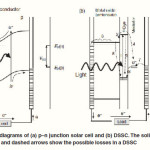
DSSCs provide a technically and economically credible alternative concept to the current p–n junction photovoltaic devices. Fig. 1(a) and 1(b) schematically depict the working process in conventional solar cells and DSSCs, respectively. For the conventional p–n junction photovoltaic devices (Fig. 1(a)), the electrons are excited to the conduction band of the semiconductor upon light absorption. The generation rate of electron–hole pairs as a function of distance from the semiconductor surface alters with the wavelength of light due to the change in the absorbance. The electrons transfer from p to n side in the semiconductor, while holes generated on the absorption move to the p-type region. The expected voltage is the difference between the Fermi levels of p and n regions. Thus, the semiconductor assumes both tasks of light absorption and charge carrier transport.
In contrast, the scheme of electron energy transfer for DSSC is different from that of the p–n junction solar cells. The reaction scheme consists of some steps as shown in Fig. 1(b):
Absorption of photon, which is determined by the absorption spectrum of the dye as well as the intensity of solar radiation spectrum.
Interfacial electron transfer (electron injection) from the adsorbed dye to the conduction band of a semiconductor.
Deactivation of the photoexcited dye, where the solar energy is lost as heat (nonradiative deactivation) or light (radiative deactivation).
Back-transfer to the mediator in the electrolyte.
Charge recombination at the dye– semiconductor interface. The electrons transferred to the conduction band will diffuse to the oxidized dye located at the surface.
Electron transport through the conduction band of the semiconductor photoelectrode to the conducting electrodes, which may be controlled by the diffusion coefficient of the electron, Dn, in the semiconductor.
Reduction of the oxidized form of the redox mediator (I3-) at the counter electrode to the reduced form (I-). For the next step, the formed I- should diffuse to the surface of the dye-attached metal oxide electrode.
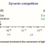
Electron transfer to the oxidized dye from a redox mediator in the electrolyte (I–) to generate the oxidized form of the redox mediator (I3-). For step (7), the generated I3- should diffuse to the surface of the counter electrode. One can see the timescale of each step in Fig. 2.33
To maintain the process of electron generation, a dynamic competition of these processes may take place. In this process, the steps indicated with broken lines (3–5) should be slow as compared to the steps (2, 6–8). As shown in Fig. 2, the electron migration across the nanocrystalline film (6) and the redox capture of the electron by the oxidized relay (7) take place within milliseconds. Since the square root of the product of the electron lifetime and the diffusion coefficient corresponds to the diffusion length of the electron, all the photogenerated carriers will be collected if the diffusion length is larger than the film thickness.
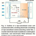
Dye sensitized photoelectrochemical solar cells have been subject of intensive research in the last years 9. Such a cell consists of a nanoporous working electrode formed by a sintered film of metal oxide semiconductor nanoparticles with a thickness of several micrometers which serves as electron acceptor and transport layer coated with a monolayer of a dye for light absorption and electron injection into the conduction band of metal oxide. An electrolyte solution, either acetonitrile or a mixture of ethylene/propylene carbonate containing the redox couple iodide/triiodide carbonate containing the redox couple iodide/ triiodide as depicted in Figure 3. Power conversion efficiencies of 10-11 % have been reported.34-36
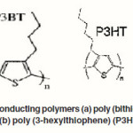
Although these cells show high power conversion efficiencies, their commercial applications are still limited due to stability problems as well as technological aspects of the large module production. The presence of a liquid electrolyte makes the manufacturing process difficult. Therefore, recent efforts in dye sensitized solar cell research are more focusing on replacing the liquid electrolyte with a solid material to eliminate practical problems with sealing. A solid state cell exhibits a structure similar to the dye sensitized photoelectrochemical cells except for the replacement of electrolyte with a p-type semiconductor or organic hole conductor material.37-40 One of the major differences between dye sensitized solar cells with liquid electrolytes and solid state device lies in the nature of charge transport: in the former case ionic transport is controlled by diffusion whereas in the latter case electronic transport, influenced by conductivity and charge transport mobility, plays an important role.41 Polymeric materials are of practical interest as replacement for the electrolyte since they are inexpensive and can be tailored chemically to fit a wide range of technological purposes. Several conducting polymers shown in Figure 4 (a) and (b) such as, poly (bithiophene) (P3BT), poly (3- hexylthiophene) (P3HT) have already been used in solid state dye sensitized solar cells.42-45
Solid-State Polymer/Inorganic Hybrid Dye Sensitized Solar Cell
Compared to dye-sensitized solar cells, the solid nanostructured metal oxide-polymer solar cell has the advantage of utilizing the complete heterostructures for exciton dissociation, potentially leading to thinner devices, since the entire polymer- filled pore volume is available for exciton generation, rather than only a dye monolayer at the metal oxide surface. Further, the rigid structure of metal oxides offers better mechanical stability compared to the organic PVs. The porous structure of nanostructured metal oxide has been investigated as an electron acceptor layer with organic photoactive polymers as the hole conductor extensively. In dye sensitized solar cells organic or complex dyes are generally used to sensitize metal oxide semiconductor (e.g., SiO2, ZnO, TiO2), where the polymers function as a hole transporter to absorb light. The power conversion efficiency of about 5.13% has recently been achieved. ZnO is a direct wide bandgap (3.3 eV at 300 K) II–VI compound semiconductor. ZnO can be grown with simple crystal-growth technologies, resulting in potentially lower costs for ZnO-based devices. High-quality ZnO films can be grown at relatively low temperatures less than 700ºC. Further, there are additional properties that make ZnO preferable over other wide bandgap materials. Impurity-created states resulting in enhanced optical absorption at lower energies would be another potential area of interest. A completely different approach on the use of ZnO in organic systems was reported by Gilot et al. They suggested that insertion of an optical spacer into the devices is another approach to increase the total thickness of active layer. The thickness of the device with an optical spacer is not good enough to trap all the incident photons. But, the light intensity inside the device was spatially redistribution due to optical interference effect and it results in enhancing device performance. Over the past few years, research into fabrication techniques for nanocrystals has led to rod-like structures (nanorods) with diameters that range from 2 to 10 nm and lengths ranging from 5 to 100 nm. Due to their intrinsic structural anisotropy, nanorods possess many unique properties that make them potentially better nanocrystals than quantum dots for photovoltaics.
Review Of Hybrid Solar Cell Using Zno
So far, various ZnO nanostructures have been extensively investigated for Solar Cells. In the early reports on ZnO-based DSSCs, ZnO nanoparticles were often used as the photoanode prepared by a conventional doctor blade technique (Keis et al., 2002; Keis et al., 2002). Law et al. (2005) presented first the ordered nanowire DSSC. The nanowire DSSC is an exciting variant of the most successful of the excitonic photovoltaic devices. As an ordered topology that increases the rate of electron transport, a nanowire electrode may provide a means to improve the quantum efficiency of DSSCs in the red region of the spectrum, where their performance is currently limited. Law et al. (2006) described the construction and performance of DSSCs based on arrays of ZnO nanowires coated with thin shells of amorphous Al2O3 or anatase TiO2 by atomic layer deposition. Wu et al. (2007) employed mercurochrome and N3 dyes to be the sensitizers in the ZnO nanowire DSSCs. Hsueh et al. (2007) deposited p-Cu2O onto vertical n-ZnO nanowires prepared on ZnO:Ga/glass templates. With the sputtered Cu2O, the nanowires became club like (i.e. nanowire with a head). Leschkies et al. (2007) combine CdSe semiconductor nanocrystals (or quantum dots) and single-crystal ZnO nanowires to demonstrate a new type of quantum dot-sensitized solar cell. A significant improvement of the efficiency of the ZnO nanowire DSSC has been achieved by the chemical bath deposition of the dense nanoparticles within the interstices of the vertical ZnO-NW anode (Ku et al., 2007). Greene et al. (2007) evaluated an ordered organic-inorganic solar cell architecture based on ZnO-TiO2 core-shell nanorod arrays encased in the hole-conducting polymer P3HT. Chen et al. (2009) studied a two-stage growth of a ZnO hierarchical nanostructure consisting of ZnO nanorod at bottom and ZnO nanowire atop in the low pH solutions. Chen et al. (2009) reported vertically aligned zinc oxide (ZnO) nanorod arrays coated with gold nanoparticles have been used in Schottky barrier solar cells. Briseno et al. (2010) demonstrated the basic operation of an organic/inorganic hybrid single nanowire solar cell. End-functionalized oligo and polythiophenes were grafted onto ZnO nanowires to produce p-n heterojunction nanowires. Gan et al. (2010) prepared hybrid ZnO/ TiO2 photo-anodes for dye-sensitized solar cells by combining ZnO nanowire arrays and TiO2 nanoparticles with the assistance of the ultrasonic irradiation assisted dip-coating method. Myung et al. (2010) synthesized high-density ZnO-CdS core- shell nano-cable arrays by depositing CdS outer- layers on pre-grown vertically aligned ZnO (wurtzite) nanowire arrays using the chemical vapor deposition method. Seol et al. (2010) a novel CdSe/ CdS/ZnO nanowire array fabricated by a 3-step solution-based method was used as a photoanode of a quantum dot sensitized solar cell, which generated a maximum power conversion efficiency of 4.15%. Wu et al. (2010) reported a 74% enrichment of the efficiency of ZnO nanowire DSSCs is achieved by the addition of a novel light scattering nanocrystalline film.
State-Of-The-Art In Solid-State Polymer/Inorganic Hybrid Dye Sensitized Solar Cell
Dye cells have three major parts, a porous layer of metal-oxide [titanium dioxide (TiO2)] nanoparticles, a monolayer of dye that covers the particles, and a¯hole-transporter that infiltrates the pores within the transparent conducting oxide (TCO) layer. TCO (e.g., TiO2, ZnO) have been used for several decades as a white powder pigment worldwide. A porous layer, or more specifically a- mesoporous layer, because the particle’s sizes range from 10 to 50 nm, is needed within the structure to provide a large surface area onto which the dye will adsorb. The dyes in the highest efficiency cells are based on ruthenium, another rare earth metal, though considerable effort is being made to transition to organic dyes such as porphyrin dyes, the class chlorophyll dyes are in, or “donor–acceptor” dyes, named for the electronic functionality of the molecule’s components. The hole-transporting material (HTM) is made of an iodide/triiodide liquid electrolyte in the highest performing cells, though steps are being made to incorporate solid HTMs instead, due to the thermal instability of liquids and the problems posed for sealing by thermal expansion. Both polymers and small molecules are being examined for their use in solid state dye-sensitized solar cells. 2,2’,7,7’- tetrakis-(N,N-di-pmethoxyphenylamine)9,9’- spirobifluorene (spiro-OMeTAD) and conducting polymers like poly (3-hexylthiopene) (P3HT) are the most widely used solid-state hole conductors.
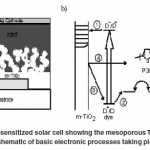
The dye-sensitized cell begins to perform when a dye molecule attached to the metal oxide (e.g., titania) surface absorbs a photon. The molecule becomes excited and an electron makes an energetic transition from the ground-state highest occupied molecular orbital (HOMO) to an excited state, the lowest unoccupied molecular orbital (LUMO). Energetically, the LUMO of the dye needs to be higher than the conduction band of the metal oxide such that injection from the dye to metal oxide is favored. Though TiO2 is an insulator and not typically thought of as a material well-suited to conducting charge, the large band gap allows electrons to flow relatively freely within its conduction band. Meanwhile, the dye cation is regenerated by electrons from the hole-transport material, P3HT, and the hole diffuses through this layer to the cathode, completing the circuit. Recombination processes occur when electrons and holes meet and release energy, reducing the cell’s efficiency. A diagram of a complete dye- sensitized cell and a scheme of electronic processes occurring in the cell are presented in Fig. 5.
In Fig 5 b, the x-axis corresponding roughly to vertical displacement in the cell shown in a) and the y-axis corresponding relatively to energy levels with respect to vacuum; 1) after absorbing a photon, the dye injects an electron in the conduction band of the TiO2;2) the hole from the oxidized dye transfers into the hole-transporter, a step equivalent to the regeneration of the dye with electrons from the hole- transporter; 3) and 4) are unfavorable processes in which electrons from the conduction band of TiO2 recombine with either the oxidized dye or holes in the polymer, respectively. Adapted from Snaith, Schmidt-Mende, 2010.46
Figure 5: a) A complete dye-sensitized solar cell showing the mesoporous TiO2, the dye, and the
hole-transporter, P3HT. b) A schematic of basic electronic processes taking place in a dyesensitized cel.
Enhancement of Photoresponse Through Interaction of Near-IR Dyes and The Polymer Hole- Transport Material
The photoresponse of solid-state dye- sensitized cells can be extended by the incorporation of polymers like P3HT because P3HT can plausibly act as both a hole-transporter and a light absorber—P3HT is red, The goal is to take advantage of a resonant energy transfer (FRET) process that would be expected to occur if the absorbance spectrum of the dye correctly overlaps with the photoluminescent spectrum of the P3HT and the molecules are within several nanometers of one another. It is known that P3HT photoluminescence at around 725 nm, though the number of dyes with such a small band gap is very low, which presents a challenge to experimentation. If both the P3HT and the dye absorb light and the P3HT serves as an antenna, relaying the energy absorbed to the dye, with the dye injected the electrons into the metal oxide mesostructure, clear panchromatic response could be reasonably attained and efficiencies for solid-state devices markedly improved.
Characterization of Polymer/Metal Oxide Hybrid Dye Sensitized Solar Cell Performance
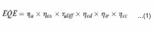
Solar cell is a device that produces electricity from sunlight. Upon illumination, photons are absorbed by an active layer in a solar cell, and then electron-hole pairs are generated as excitons. The excitons need to diffuse to a donor–acceptor (DA) interface to dissociate into free charges. After that, electrons and holes need to transport to electrodes through their corresponding percolation pathway.57 During these processes, six main steps affect device performance : i) photon absorption (sa); ii) exciton generation (sex); iii) exciton diffusion (sdiff); iv) exciton dissociation (sed); v) charge transport (str); vi) charge collection (scc). The h is the yield of each process. These six processes determining a solar cell performance can be better understood in a connection with external quantum efficiency (EQE) of a device. EQE is defined as a percentage of the number of charge carriers collected at the electrode under short-circuit condition to the number of photons incident on the device58 EQE can be expressed as the product of the above steps.
Solar cell efficiency can be calculated from its current density voltage (J-V) characteristic curves. From such curves, open-circuit voltage (Voc), short-circuit current density (Jsc) and fill factor (FF) can be obtained. Then energy conversion efficiency can be determined by:

Where Ps is the incident light power density
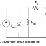
Equivalent circuit of a solar cell is shown as Fig. 6. A series resistance Rs originates from contact and bulk semiconductor, and a shunt resistance Rsh comes from poor diode contact.47 The J-V characteristics can be described as.48
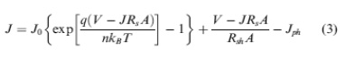
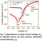
Where kB is Boltzmann’s constant, T is temperature, q is elementary charge, A is device area, n is ideality factor of the diode, J0 is reverse saturation current density, Jph is photocurrent, Rs is series resistance and Rsh is shunt resistance. The J-V curves and photovoltaic parameters including Voc and FF strongly depend on the n, J0, Rs, and Rsh. Fig. 7 shows typical dark and illuminated current density-voltage (J-V) curves, in which three distinctive regions can be seen.49 The first (I) is the linear region in negative potentials and low positive potentials, in which the current density is dominated by the shunt resistance (Rsh). The second (II) is the region at mediate positive regions where the curve shows an exponential behavior and the current density is related to the diode. The third (III) is another linear region in high positive potentials where the current density is related to the series resistance (R ).49 The ideality factor (n) is a figure 7 which shows how closely a diode behaves like an ideal diode and it is typically deviated from the ideal by recombination in the junction.50
Fig. 7: Dependence of open circuit voltage (Voc) on ideality factor (n) and reverse saturation current density (J0).
The reverse saturation current density (J0) is also an important parameter affecting the J-V curves in the exponential regimes and thus cell performance. The J0 is an indicator of how many charges can overcome the energetic barrier in the reverse direction. These charges are regarded as minority charges at the donor/acceptor interface. In a typical p-n junction, J0 can be described as49-51-52
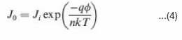
Where Ji depends on material purity and x is energetic barrier voltage. x was found to be in good agreement with energy difference of the acceptor’s LUMO and the donor’s HOMO. The J0 value increases with increasing temperature (T), but decreases as the material quality (purity) and energetic barrier improve.The series resistance (R ) is another parameter that affects the J-V characteristics and solar cell performance. The Rs results from limited conductivity of organic layer,contact resistance between organic layer and its corresponding electrodes, and connecting resistance between the electrodes and external circuit. The Rs can reduce the FF and it can also reduce the Jsc if it is too high. Generally the Rs has no impact on open circuit voltage (Voc) since the entire current flows through the diode at the Voc condition, but no current flows though the Rs. However, at the points close to the Voc, the Rs greatly affect the J-V curves, providing a simplified method to estimate the Rs by measuring the slope of the J-V curves in the regime close to the Voc.50 The R should be minimized to reduce the energy loss, especially in large area solar cells 49-52. The shunt resistance (Rsh) is also a parameter affecting the J-V characteristics and solar cell performance. The Rsh may be related to the device structure and film morphology. For example, Rsh can be lowered by the leakage current through the pinholes and recombination of charge carriers in the devices.53 The morphology and thickness can be processed with care to reduce the pinholes and recombination in the devices so that the Rsh can be increased. The Rsh needs to be maximized to reduce the power loss caused by the current that bypasses the solar cell junction and load through an alternate current path from the low Rsh. A small Rsh lowers the current flowing through the diode (junction) and thus reduces the Voc. A simplified way to approximately calculate the Rsh is to measure the slope of the J-V curves in the regime close to the Jsc.50 The above
discussed n, J0, Rs and Rsh can strongly affect the photovoltaic parameters including Voc , FF, Jsc and cell efficiency (h). Voc is defined as the voltage across the cell under illumination with a zero current at which the dark current and short circuit photocurrent was exactly cancelled out.54 By solving the current density verse voltage equation (eq 3), Voc can be derived as:
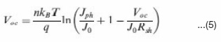
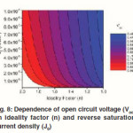
Fig. 8 shows the dependence of Voc on n and J0, calculated using eq. 6 that is derived from eq. 5 by assuming an infinitely large Rsh. It can be seen that the decrease of J0 and increase of n can significantly increase the Voc.
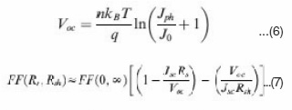
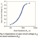
When the Rsh is not large enough, it can also affect the Voc of Polymer–inorganic hybrid solar cells. Figure 9 shows the dependence of Voc on the Rsh plotted using eq 5. The FF is greatly affected by the Rs and Rsh. The relationship has been reported previously.55 High FF can be achieved with low R and high Rsh. Therefore, the Rs needs to be minimized and the Rsh should be maximized to ensure a high FF.
Figure 6: Equivalent circuit of a solar cell
Figure 7: Dependence of open circuit voltage (Voc) on ideality factor (n) and reverse saturation
current density (J0).
Figure 8: Dependence of open circuit voltage (Voc) on ideality factor (n) and reverse saturation current density (J0).
Figure 9: Dependence of open circuit voltage (Voc) on shunt resistance (Rsh).
Polymer–inorganic hybrid solar cells have gained extensive attention and recent research progress. While power conversion efficiencies exceeding 3% have recently been achieved for polymer–inorganic hybrid solar cells, these efficiencies are still lower than those of polymer- fullerene solar cells, which have recently reached as high as 8.13%. In physically blended polymer– inorganic hybrid solar cells, although charge separation has improved. To resolve poor electron transport, pre-synthesized inorganic nanostructures have been used to either infiltrate the polymers or in situ polymerize donor materials within the nanopores. Among these approaches, ordered nanostructures are considered an ideal configuration for achieving high efficiency utilizing one dimensional (1-D) inorganic semiconductors to realize continuous charge transport pathways.56 minimized and the Rsh should be maximized to ensure a high FF.To further improve device performance of polymer– inorganic hybrid solar cells, several challenges need to be considered including morphology control, polymer and inorganic material engineering, and donor–acceptor interface modification. A more efficient morphology control of polymer–inorganic active layer is needed to achieve not only an effective charge separation, but also an efficient charge transport and collection. Numerous experiments have been designed and carried out to test the effects of additives and the effects of atmospheric oxygen on the conducting polymer hole-transporter, P3HT. Tests of additives in devices have confirmed and in some cases optimal concentrations have been determined. A fairly highly efficient device concept for solid-state hybrid dye-sensitized solar cells has been realized. The device is fabricated from inorganic nanoparticles as electron transporting material, an organic hole transport materials with photoexcited dye molecules as electron injector into the n-type material and the hole accepting and transporting properties of polymer like P3HT. Since the dye is regenerated by the hole injection in the p-type material, the operating principle of DSC based on liquid electrolyte is similar to that of solid-state hybrid DSC. It has been investigated through I-V characterization that the device shows open-circuit voltages of up to 550 mV and short circuit currents up to 11mA/cm2. The results show the usefulness of conducting polymers as hole transport materials for the possible replacement of the liquid electrolyte in nanoporous metal oxide semiconductor type solar cells and optimization of these devices is a promising approach from both academic and industrial sides. These advances are a testimony to the rapid progress being made in the field of DSCs and to the promise they hold for growing into a viable technology as a low-cost renewable energy source. Several challenging scientific and technological problems, however, remain to be solved. The major problems associated with solid- state cells seem to be the imperfect filling of a transparent hole conductor into the pores between the nanoparticles and the nature of the contact between the p-type semiconductor and the dye monolayer.
References
- Jager-Waldau, European Commission, PV Status Report 2003, EUR 20850 EN (2003).
- S.-S. Sun and N. S. Sariciftci, Organic photovoltaics: mechanisms, materials, and devices, CRC Press, Boca Raton (2005).
- Becquerel E. C R Acad. Sci. Paris, 9: 561 (1839).
- F. C. Krebs, T. D. Nielsen, J. Fyenbo, M. Wadstrom and M. S. Pedersen, Energy Environ. Sci., 3: 512–525 (2010).
CrossRef
- Perlin. From Space to Earth–The story of solar Electricity. Ann Arbor, MI: AATEC Publications; (1999).
- Sun S, Fan Z, Wang Y and Haliburton J., Organic solar cell optimization. J Mater Sci., 40: 1429–43 (2005).
CrossRef
- Chapin DM, Fuller CS and Pearson GL., J. Appl. Phys., 25: 676 (1954).
CrossRef
- C. Brabec, N. S. Sariciftci and J. C. Hummelen,Adv. Func. Mat. 11: 15 (2001)
CrossRef
- B. O’Regan and M. Grätzel, Nature. 353: 737 (1991).
CrossRef
- J. Krüger, R. Plass, M. Grätzel, and H. J. Matthieu, Appl. Phys. Lett. 81: 367 (2002).
CrossRef
- P. Taranekar, Q. Qiao, J. Jiang, K. S. Schanze and J. R. Reynolds, J. Am. Chem. Soc., 129: 8958–8959 (2007).
CrossRef
- Q. Qiao, Y. Xie and J. J. T. McLeskey, J. Phys. Chem. C, 112: 9912–9916 (2008).
CrossRef
- S. B. Darling, Energy Environ. Sci., 2: 1266– 1273 (2009).
CrossRef
- Roberson LB, Poggi MA, Januszkowalik, Smestod GP, Bottomley LA, Tolbert LM.,Coord. Chem. Rev., 248: 1491–7 (2004).
CrossRef
- W. Beek, M. Wienk and R. Janssen, Adv.Mater., 16: 1009–1013 (2004).
CrossRef
- W. J. E. Beek, M. M. Wienk, M. Kemerink, X. Yang and R. A. J. Janssen, J. Phys. Chem. B, 109: 9505–9516 (2005).
CrossRef
- J. Liu, W. Wang, H. Yu, Z. Wu, J. Peng and Y. Cao, Sol. Energy Mater. Sol. Cells, 92: 1403– 1409 (2008).
CrossRef
- M. D. Goodman, J. Xu, J. Wang and Z. Lin,Chem. Mater., 21: 934–938 (2009).
CrossRef
- J. Boucl_e, S. Chyla, M. S. P. Shaffer, J. R. Durrant, D. D. C. Bradley and J. Nelson, Adv. Funct. Mater., 18: 622–633 (2008).
- P. Ravirajan, A. M. Peiro, M. K. Nazeeruddin,M. Graetzel, D. D. C. Bradley, J. R. Durrant and J. Nelson, J. Phys. Chem. B, 110: 7635– 7639 (2006).
CrossRef
- A. M. Peiro, P. Ravirajan, K. Govender, D. S. Boyle, P. O’Brien, D. D. C. Bradley, J. Nelson and J. R. Durrant, J. Mater. Chem., 16: 2088– 2096 (2006).
CrossRef
- Y. Wu and G. Zhang, Nano Lett., 10: 1628– 1631 (2010).
CrossRef
- K. M. Coakley and M. D. McGehee, Chem. Mater., 16: 4533–4542 (2004).
CrossRef
- H. Borchert, Energy Environ. Sci., 3: 1682– 1694 (2010).
CrossRef
- I. Gonzalez-Valls and M. Lira-Cantu, Energy Environ. Sci., 2: 19–34 (2009).
CrossRef
- Y. Zhou, M. Eck and M. Kruger, Energy Environ. Sci., DOI: 10.1039/C0EE00143K (2010).
CrossRef
- S. G•unes and N. S. Sariciftci, Inorg. Chim. Acta, 361: 581–588 (2008).
- M. Helgesen, R. Sondergaard and F. C. Krebs,J. Mater. Chem., 20: 36–60 (2010).
CrossRef
- J. Boucl_e, P. Ravirajan and J. Nelson, J. Mater. Chem., 17: 3141–3153 (2007).
- S. Dayal, N. Kopidakis, D. C. Olson, D. S. Ginley and G. Rumbles, Nano Lett., 10: 239– 242 (2010).
CrossRef
- R. Zhu, C.Y. Jiang, B. Liu and S. Ramakrishna,Adv. Mater., 21: 994–1000 (2009).
CrossRef
- J. A. Chang, J. H. Rhee, S. H. Im, Y. H. Lee, H.-j. Kim, S. I. Seok, M. K. Nazeeruddin and M. Gratzel, Nano Lett., 10: 2609–2612 (2010).
CrossRef
- Graetzel M., J. Photochemistry and Photobiology A. 164: 3–14 (2004).
CrossRef
- M.K. Nazeeruddin, A. Kay, I. Rodicio, R. Humphrybaker, E. Muller, P. Liska, N. Vlachopoulos and M. Grätzel, J. Am. Chem. Soc., 335: 6382 (1993).
CrossRef
- C.J. Barbe, F. Arendse, P. Comte, M. Jirousek,F. Lenzmann, V. Shklover and M. Grätzel, J. Am. Chem. Soc., 80: 3157 (1997).
- M. A. Green, K. Emery, K. Bücher, D. L. King and S. Igari, Prog. Photovolt. Res. Appl., 6: 35 (1998).
CrossRef
- A.F.Nogueira, C. Longo and M.A. De Paoli, Coord. Chem. Rew. 248: 1455 (2004).
CrossRef
- A. Fujishima and X.T. Zhang, Proc. Jap. Acad. B, 2: 33 (2005).
CrossRef
- B. Li, L. Wang, B. Kang, P. Wang and Y. Qiu, Sol. En. Mat. Sol. Cells, 90: 549 (2006).
CrossRef
- D.Gebeyehu, C. Brabec, N. S. Sariciftci, D. Vangeneugden, R. Kiebooms, D. Vanderzande, F. Kienberger and H. Schindler, Synth. Met., 125: 279 (2002).
CrossRef
- B. Peng, G. Jungmann, C. Jäger, D. Haarer,H.W. Schmidt and M. Thelakkat, Coord. Chem. Rev., 248: 1479 (2004).
CrossRef
- G. Smestad, S. Spiekermann, J, Kowalik, C.D. Grant, A. M. Schwartzberg, J. Zhang, L. M. Tolbert and E. Moons, Sol. En. Mat. and Sol.Cells, 76: 85 (2003).
CrossRef
- L. Sicot, C. Fiorini, A. Lorin, J.M. Nunzi, P. Raimond and C. Sentein, Synth. Met., 102: 991 (1999).
CrossRef
- D. Gebeyehu, C.J. Brabec and N.S. Sariciftci, Thin Solid Films, 403: 271 (2002).
CrossRef
- C. Zafer, C. Karapire, S. Icli, Sol. En. Mat. Sol. Cells, 88: 11 (2005).
CrossRef
- Snaith, H. J.; Schmidt-Mende, L., Adv. Mater.,19: 3187–3200 (2007).
CrossRef
- J. C. BERN_EDE, J. Chil., Chem. Soc., 53: 1549–1564 (2008).
- P. Schilinsky, C. Waldauf, J. Hauch and C. J. Brabec, J. Appl. Phys., 95: 2816–2819 (2004).
CrossRef
- C. Waldauf, M. C. Scharber, P. Schilinsky, J.A. Hauch and C. J. Brabec, J. Appl. Phys., 99: 104503 (2006).
CrossRef
- C. Honsberg and S. Bowden, http:// pvcdrom.pveducation.org/.
- P. Schilinsky, C. Waldauf and C. J. Brabec,Adv. Funct. Mater., 16: 1669–1672 (2006).
CrossRef
- B. Kippelen and J.L. Bredas, Energy Environ. Sci., 2: 251–261 (2009).
CrossRef
- W. J. Potscavage, A. Sharma and B. Kippelen,Acc. Chem. Res., 42: 1758–1767 (2009).
CrossRef
- J. Nelson, The Physics of Solar Cells, Imperial College Press, London (2003).
- B. P. Rand, J. Genoe, P. Heremans and J. Poortmans, Progr. Photovolt., Res. Appl., 15: 659–676 (2007).
CrossRef
- A. L. Briseno, T. W. Holcombe, A. I. Boukai, E.C. Garnett, S. W. Shelton, J. J. M. Frecchet and P. Yang, Nano Lett., 10: 334–340 (2010).
CrossRef
- M. K. Siddiki, J. Li, D. Galipeau and Q. Qiao,Energy Environ. Sci., 3: 867–883 (2010).
CrossRef
- B. R. Saunders and M. L. Turner, Adv. Colloid Interface Sci., 138: 1–23 (2008).
CrossRef