Design of Log Periodic Dipole Array (Lpda) with Cross-shape Eaching for Uhf-vhf Application (200-1500mhz) With Band Notch of (800mhz -1000mhz)
Mahmoud Hezari*
Electronics and Mechanical Department, Pune University, India
DOI : http://dx.doi.org/10.13005/msri/090211
Article Publishing History
Article Received on : 25 Oct 2012
Article Accepted on : 05 Dec 2012
Article Published :
Plagiarism Check: Yes
Article Metrics
ABSTRACT:
Computer analysis reveals that the anomalous behavior of symmetric Log Periodic Dipole Array (LPDA)Antennahas infloenced by different parameters . The most important is mainly due to the radiation of the dipole elements in the anomalous radiating region which is excited by the transmission line resonance of the feed structure. In the design by changing the element spacing , changes of length of each element in the LPDA antenna and define cross eaching in an boom of an antenna in middle of the specified element the result is the return loss less from 200 MHZ to 1500 MHZ other than the notch between 850 MHZ 950 MHZ according to the simulation results.The log-periodical Dipole Antenna (LPDA) is a kind of ultra wide-band antennas. To achieve the purpose of miniaturization of the LPDA in radiate direction, this paper presents anunusual structure log-periodically loaded with slot cross-shape design.
KEYWORDS:
Ultra wideb and Antenna; LPDA; Notch
Copy the following to cite this article:
Hezari M. Design of Log Periodic Dipole Array (Lpda) with Cross-shape Eaching for Uhf-vhf Application (200-1500mhz) With Band Notch of (800mhz -1000mhz). Mat.Sci.Res.India;9(2)
|
Copy the following to cite this URL:
Hezari M. Design of Log Periodic Dipole Array (Lpda) with Cross-shape Eaching for Uhf-vhf Application (200-1500mhz) With Band Notch of (800mhz -1000mhz). Mat.Sci.Res.India;9(2). Available from: http://www.materialsciencejournal.org/?p=1134
|
Introduction
Log-periodic dipole antenna array have advantage of self-similar structure,its electrical properties iterate periodically with logarithm of frequency.high-performance UWB antennas require impedance matching ,efficiency, low signal distortion within thespecified frequency bands1-3. The term notch is define here as the specific eatching that make change in radiation, directivity and efficiancy of antenna4. There are many existing wireless communications systems, which are located at the frequency band overlapping to that of the UWB systems. The UWB systems will cause interferences to these systems such as IEEE 802.11a in USA (5.150 GHz–5.350 GHz and 5.725 GHz–5.825 GHz), HIPERLAN/2 in Europe (5.150 GHz–5.350 GHz and 5.470 GHz– 5.725 GHz), and World Interoperability for Microwave Access (WiMAX) (3.400 GHz–3.690 GHz and 5.250 GHz–5.825 GHz)5. Thus, designing UWB antennas with multiple frequency notched bands for blocking the interference between the UWB systems and the existing narrow bandwireless communication systems has become a challenge research topic6,7. Frequency bands allocated to various types of radio services in India but for mobile communication in Mhz 806-960 Used by GSM and CDMA mobile services(In India GSM technology works in the frequency bands of 900 and 1800 MHz and CDMA technology works in the 800 MHz band)4.
Design consideration the LPDA
CST2102 antenna design software uses a wire antenna of a constant diameter for each element to calculate antenna characteristics. Actually, the Log Periodic Dipole Array antenna can be determine by the following equation :
In the first step, the scale factor, spacing factorand the number of the dipole elements should be determined.The longest element length in LPDA is given by
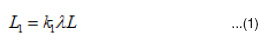
where λL is the longest operating wavelength and K1 is the lower truncation constant. We determine K1 from the empirical equation
Wavelength at 200MHz: λ = 150cm, shortest operating wavelength.
Wavelength at 1500MHZ: λ = 20cm , longest operating wavelength.
K1 = 1.01 – 0.519τ ….(2)
We calculate the upper truncation constant from
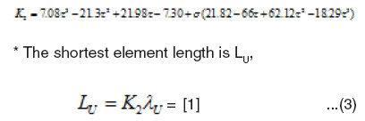
where λU is the shortest operating wavelength.
The value of LU=4.866 cm that is calculated from the equation (3). By using the truncation constants and the frequency band edges for calculating the number of dipole required for the a specify design
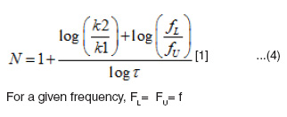
The number of element for the design from Eqn(4) is,To reach to better result adding the number of element by 2 make the total number of element comes to 27 element we compute the number of elements in the active region from equation(5) then we get,
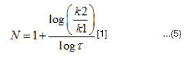
the no. of element in active region is counted as 10. By increasing the number of elements in the active region we get increases in a gain of LPDA even we can say gain have a perpendicular relation with log τ.
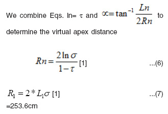
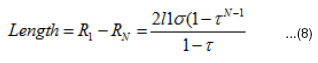
The axial length of the antenna is the difference between R1 and RN :
Finally, once the dimensions of the longest dipole element are determined, the dimensions of other dipoles can becompute the dimensions of the antenna from the equations by using an integer number of dipoles ,for better implementations in practical for number of element the diameter of dipole has holed the same so practically it will be easier6.
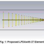
Fig. 1 shows the layout of the proposed LPDA. It consists of 26 dipole elements. This antenna is defined as reference antenna for the comparison.
Figure 1: Proposed LPDAwith 27 Element
In Table .1describe the parameters of the LPDA obtained by fine optimizing the dimensions of the LPDA with the goal of impedance matching within the standard UWB frequency band.
Table 1: Parameters of LPDA
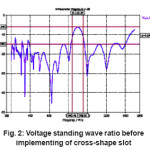
The simulated voltage standing wave ratio (VSWR) of the LPDA before implementing of crossshape slotis shown in Fig. 2.
Figure 2: Voltage standing wave ratio before implementing of cross-shape slot
Design issue of the cross-shape slot
To realize band-notched characteristic, band-stop filter should be incorporated into the antenna design. A shunt open circuit stub is the simplest way to realize the band-stop effect. However, the shunt connection will occupy booms area. For the notched band antenna design,shunt open circuit stub with the length should be used, but it will result in strong mutual coupling between the stub, which leads to the increase of design complexity.
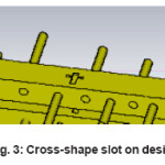
In this paper, cross-shaped slotare used to create notched band instead of shunt open circuit stub. Compared to other shaped slot ,cross-shaped slot has more flexibility to choose the location and more cross-shaped slot can be easily inserted into the pro-posed LPDA[5]. Due to the mechanism of LPDA, the location of cross-shaped slot should be prior to the resonated dipole element in order to obtain better band-notched performance. Fig. 3 shows the proposed LPDA incorporated with a cross-shaped slot, which can be equivalent to the shunt open circuit stub but with much compact layout. The physical length of the cross-shaped slotis about cross-wavelength at the notched frequency such that the slot resonates and stops the signal. Total signal reflection is expected at the notched frequency.
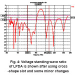
Voltage standing wave ratio(VSWR) of the LPDA is shown after using cross shape slot and some minor changes in Fig. 4.
Figure 3: Cross-shape slot on design
Figure 4: Voltage standing wave ratio of LPDA is shown after using cross -shape slot and some minor changes
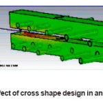
Figure 5: Effect of cross shape design in an antenna
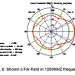
Figure 6: Shown a Far-field in 1200MHZ frequency
Conclusion
The purpose of this study is to gain more complete understanding of the LPDA antenna with goal of developing and notch bandwidthwith optimized design procedure.
This is achieved by making distance between the elements on resonating region as well as changes on width of elements, this discussion consider more in defining an cross-shape slot to gain better VSWRin design a band of 800MHZ to 1000MHZ. Following the development of the design procedure mention above ,successfully designed log- periodic antenna for frequency independent operation with range of 200-1500MHZ, An average of -14 dB of S11 is obtained over the entire bandwidth other than a notch band. Results indicate that the notch can be implemented in LPDA, if proper care is taken while fabricating the mechanical structure of the antenna .
References
- Balmain, et al, “Asymmetry phenomena of log periodic dipole antenna” IEEE Transaction on Antenna & Propagation, 24(4): (2003).
- Deshpande,A.A. “PRI-GBT Multi-Band Receiver and Pulsar-Emission-Cone Tomography”. IEEE: 9 (2011).
- Guo, et al. “A band-notched UWB Log dipole antenna fed by strip line”. IEEE:1,2010
CrossRef
- J. Kraus and R. Marhefka. Antennas .McGraw-Hill (2001).
- Jiang, et al. . “Compact Ultra- Wideband Directional printed Antenna with Notched Band”. IEEE:5 (2011).
- Patil, et al. “ Design of a wideband dualfrequency notched micro strip antenna”. IEEE: 2 (2006).
- W. Stutzman and G. Thiele. Antenna Theory and Design, , Wiley (2008).

This work is licensed under a Creative Commons Attribution 4.0 International License.