Introduction
An important and fundamental property of a semiconductor material is its dielectric permittivity which arises due to the difference in electro negativities of the constituent atoms in a binary / mixed semiconductor compound. A thorough knowledge of this parameter is essential for solving many problems in semiconductor Physics, particularly in the electric field stimulated emission studies in presence of impurities, voids, structural defects and studies on polarization and relaxation mechanisms etc.1, 2 Initially, such studies played a useful role with insulators and ferrites and later gave a strong hope with semiconductors.
Abo El Ata and Atia3 have studied ac conductivity and dielectric properties for a series of polycrystalline spinal ferrite with composition CoAlxFe2-xO4, as a function of frequency and temperature. The dispersion of the dielectric constant was discussed in the light of Koops26 model and hopping conduction mechanism. The dielectric loss tangent ( tan d ) curves exhibited dielectric relaxation peaks which were attributed to the coincidence of the hopping frequency of the charge carriers with that of the external fields. The ac conductivity, dielectric constant and dielectric loss tangent were found to increase with increase in temperature due to increase of the hopping frequency, while they decrease with increasing Al ion content due to the reduction of iron ions available for the conduction process at the octahedral sites. The material displays dielectric dispersion and a loss peak was observed. Colecole diagrams have been used to determine the distribution parameters (a) and the molecular relaxation time (t), and Eyrings relaxation rate equations are used to determine the free energy of activation. The process of dielectric relaxation (loss) and ac conduction was attributed to the correlated barrier hopping model (CBH) suggested by Elliott 4 for amorphous solids where two carriers simultaneously hop over a barrier between charge defect D+ and D– states.
Hegab5 have studied the ac conductivity and the dielectric constant for the chalcogenide glasses Te38+yAs40-yGe10Si12 (y = 0.3,6 and 7 at %) as a function of temperature (290–3830K) and frequency (102 – 105 Hz). The experimental results indicated that ac conductivity and the dielectric constant depend on the temperature and frequency and the Te content. The ac conductivity is found to obey ws law in accordance with the hopping model and s is found to be temperature dependent and its value goes down as the temperature is increased. The temperature dependence of ac conductivity was interpreted in terms of the correlated barrier hopping model (CBH).
Mustafa et al.,6 have studied the dielectric properties of undoped and doped CdTe with Ga,In, Pb prepared using the THM technique. The dielectric measurement of them have shown thermally activated properties. It is also found that the regular band type conduction is contributing to the conduction mechanism. The role of dopant was found to lower the values of the activation energy for loss mechanism. The role of dopant was found to lower the values of the activation energy for loss mechanism, which is the dominant mechanism for the observed complex permittivity and also for ac conduction.
The dielectric properties and ac conduction of the AgSbTe2 ternary semiconductor were investigated7 and found that the density of defects was found to increase with the increase in temperature which explains the increase of (tan)max and DÎ’ with temperature. Dielectric loss in ternary amorphous and liquid semiconductor AgSbTe2 can be interpreted using the charged defect D+ and D – model, where the correlated barrier hopping of bipolarons (two carrier hopping between D+ and Dstates) is made responsible for the ac conductivity mechanism.
Sadhanadevi & Prakash 8 have studied photodielectric effects in CdS-ZnO solid solution. The studies have been carried out principally on powders of ZnO and CdS separately. The magnitude of the effect varies from an increase in dielectric constant by a factor of 2-3 in CdS, to 7-100 in ZnO. Photodielectric effect is also reported for (ZnO-CdO) and HgI2:CdS systems.9,10.Dielectric properties of other materials have been investigated by several workers.11-15 Abo El Ata et al.,3 have studied the effect of Al ion substitution on the behaviour of ac conductivity and dielectric properties of CoFe2O4 at different frequencies and temperatures. They have shown how low cost, easily manufacturing and interesting electric and magnetic properties lead the polycrystalline ferrite to be one of the most important materials that has attracted a considerable attention in the field of technological application in a wide range of frequency extended from microwave to radio frequency, their electrical and dielectric properties depends on the preparation conditions, such as sintering, temperature, sintering atmosphere and soaking time as well as the type of the substituted ions. It was proposed that the air-sintered ferrites are characterized by microstructure consisting of relatively high conductive grains separated by high resistive thin layers (grain boundaries).16, 17 Most of the external applied electric field to the specimen is concentrated on the grain boundary regions, therefore the electrical properties of the grain boundary phase control the electric and dielectric properties of this materials.
Diger et al.,18 have studied the ac conductivity and dielectric properties of the amorphous Se films in the frequency range 100 Hz – 100 kHz and in the temperature range 100-4000 K. The ac conductivity σac(ω) is found to be proportional to ws where s<1. The temperature dependence of both ac conductivity and the parameter s is reasonably well interpreted by the correlated barrier model (CBH). The dc conductivity at room temperature was also studied in the same thickness range. It was concluded that the same mechanism of carrier motion might be dominant in both ac polarization and dc conduction. This carrier transport mechanism might be electronic.
Dubey et al.,19 have studied loss tangent, loss capacitance, relaxation times, ac conductance, ac capacitance for dielectrics and semiconductors in different shapes, sizes and states. Here, a new method is suggested to evaluate all the above parameter using Debye equations and measuring capacitance of phosphor cells at different audio frequencies. Relaxation time at room temperature comes out to be micro seconds. This may be due to electron traps at 0.7 eV below the conduction band.
This dielectric study leads to the same trap level position as found by many workers in thermally stimulated luminescence (TSL) and thermally stimulated conductivity (TSC) as well as phosphorescence decay mechanism.
The dielectric behaviour of (CdSe)1-x(ZnS)x depends on chemical composition and preparation conditions. While most of the work of dielectric and ac conductivity studies were focused on insulating materials20, 21, ferrites22, 23, superconductors24 etc., the theoretical aspect of model dielectric function of the binary such as CdS, CdSe and ternary CdZnTe, CdHgTe and AgSbTe2 semiconductors25-29 measured by spectroscopic ellipsometery in the photo energy range at room temperature was reported by many workers. Benguigui et. al.30 presented the new data concerning the dielectric properties of binary semiconductor solid solutions at different frequencies. Results of spontaneous polarization demonstrate that this system exhibits a diffuse, second-order ferroelectric transition. The transition is of order-disorder type as deduced from the dielectric measurements.
A detailed survey of the literature reveals that though, some work on dielectric properties has been carried out on binary semiconductor films/ bulk material3 and on some mixed semiconductors31, 32 systematic work on mixed semiconductor compounds of CdSe and ZnS is not available till date. The aim of the present work is to obtain the data related to the dielectric properties of (CdSe)1-x (ZnS)x polycrystalline semiconductor compounds since the frequency effects on the dielectric behaviour and ac. electrical conductivity offers valuable information about conduction phenomena of (CdSe)1-x(ZnS)x compounds. Hence, the dielectric measurements as a function of frequency in the range of 100Hz – 1MHz at room temperature in various samples of (CdSe)1-x(ZnS)x are reported and the results are provided necessary explanation.
Experimental
Sample Preparation
The (CdSe)1-x(ZnS)x compounds with x = 0 – 1.0 were prepared in the form of precipitate by controlled co-precipitation method. The precipitate was transferred into a clean ceramic boat and was kept in a quartz tube arranged in a high temperature tubular furnace (0-1000°C). The precipitate was dried at 300°C under Nitrogen atmosphere for 2 hours. Then the precipitate was ground in to fine powder which was made into pellets under 10 tons of pressure by using a punch die. The pellets were sintered at 800°C for 2 hours under the Nitrogen atmosphere. The pressure of the gas was maintained uniform throughout the heating process and later the furnace was cooled very slowly (1°C/ minute) to room temperature.
Measurement of Dielectric Constant at Different Frequencies
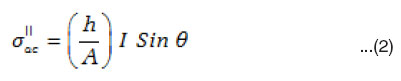
The digital multi frequency LCR meter is used to measure the a.c. voltage drop VR developed across a standard resistance R connected across the dielectric cell, frequency f and phase angle q between the voltage (V) and current ( I ) simultaneously. The standard resistance R value is adjusted to make VR very small with respect to V i.e., VR / V<<1%. The current I passing through the sample is calculated using Ohm’s Law (I = VR / R). This current consists two terms, the inphase component (I Cosq) and the out of phase component (I Sinq) from which the real (σ”ac) and imaginary (σ”ac) parts of ac. electrical conductivity are calculated using the expression.33
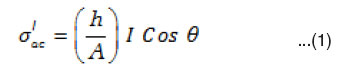
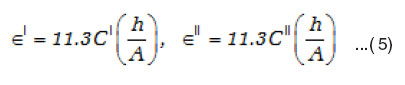
where ‘h’ is the thickness and A is the area of cross-section of sample
The real ac conductivity itself consists of two terms.
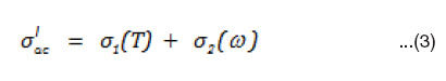
The first term σ1(T ) is frequency independent and temperature dependent is due to the drift mobility of electric charge carriers, it is actually the d.c. electric conductivity and follows an Arrhenius form. The second term σ2(ω) is frequency and temperature dependent and is related to the dielectric relaxation caused by the localized electric charge carriers.
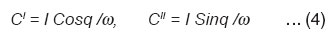
The real / imaginary components of the capacitance C of the sample (in pico farads) is calculated from the real / imaginary part of the ac current.
Therefore the real / imaginary dielectric constant ∈’/∈” is calculated from C values as
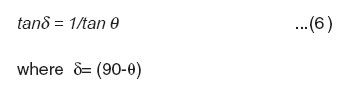
The dielectric loss tand is calculated using the relation
Distribution Parameter ( a ) and Relaxation Time (τ ) from Cole – Cole plots
Cole and Cole34 showed that if a dielectric system has a distribution of relaxation times, then the complex plane locus, obtained by plotting ∈’ versus ∈” is generally an arc of a circle intersecting the abscissa axis at the values of ∈∞ and ∈s and having its center lying below the abscissa axis where ∈s and ∈∞ are the static and optical dielectric constants. The diameter drawn through the center from ∞ makes an angle α π/2 with the ∈’ axis (α π/2) being determined from the plots and a is calculated. Knowing a, one can determine the macroscopic relaxation time t0 by using the relation
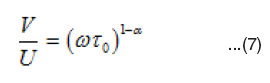
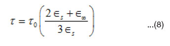
where V is the distance on the cole-cole diagram between ∈s and the experimental point. U is the distance between the point and ∈∞, and w is the angular frequency. The parameter a is equal to zero when the dielectric has only one relaxation time and larger the a larger is the extent of the distribution of the relaxation time (0 < a < 1). The molecular relaxation time (t) can be estimated from (t0) using35
Activation Energy (DF) for Dipole Relaxation
Eyring et al.36-38 has shown that the molecular relaxation time in the chemical rate theory is given by
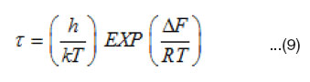
Where DF is the free energy of activation for dipole relaxation, k is Boltzmann’s constant, and h is plank’s constant. Therefore, the free energy of activation DF can be calculated from
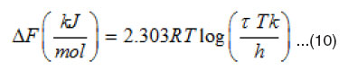
From Eqn. 10, the activation energy DF can be calculated at different concentrations.
Results and Discussion
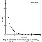
The real part of the dielectric constant (∈’) of all mixed semiconductor samples of (CdSe)1- x(ZnS)x with x = 0 – 1 measured at room temperature was found high at low frequencies and decreases rapidly with the applied frequency. The typical variation of ∈’ with frequency of the applied field in (CdSe)1-x(ZnS)x samples is represented in Fig.1.
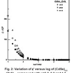
The variation of ∈’ with frequency for compounds with x = 0.2, 0.3, 1 are shown in Fig. 2. It is observed that at 3000K (room temperature) the value of ∈’ decreases from 1.42 x 10⁸ to 1.57×10⁴ in sample with x = 0.2, from 2.16×10⁸ to 2.13×10⁴ in sample with x = 0.3, from 1.72×10⁸ to 1.69×10⁴ in sample with x = 0.5, from 2.08×10⁸ to 2.05×10⁴ in sample with x = 0.7, from 2.1×10⁸ to 2.1x 10⁴ in
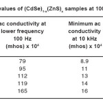
Table 1: Ac Conductivity Values of (CdSe)1-x(ZnS)x Samples at 100Hz, 10 kHz and 100 kHz
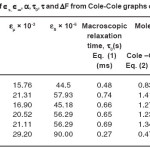
Table 2: Calculated Values of ∈s, ∈∞, α, τ0, τ and ΔF from Cole-Cole Graphs of (CdSe)1-x(ZnS)x Compounds
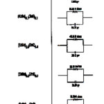
Table 3
sample with x = 0.8 and from 2.97×10⁸ to 2.92 x 10⁴ in sample with x = 1, when the frequency is changed from 100 Hz to 1MHz. This indicates that the dielectric constant at room temperature decreases with the increase in frequency in general, and at a given frequency it increases with the composition. For (CdSe)1-x(ZnS)x sample with x = 1.0, the value of the dielectric constant is high with reference to those of the other samples. Generally the decrease of dielectric constant ∈’, with the increase in frequency is similar in all (CdSe)1-x(ZnS)x samples indicating that the dispersion feature is nearly temperature independent.
The high values of ∈’ can be explained on the basis of the Maxwell-Wagner model and Koops phenomenological theory16,39,40. According to these models, the dielectric material with heterogeneous structure can be imagined as a structure consisting of well conducting grains separated by highly resistive thin layers (grain boundaries). In this case, the applied voltage on the sample drops mainly across the grain boundaries. The space charge polarization is governed by the available free charges on the grain boundary and the conductivity of the samples. Koops proposed that the effect of grain boundaries is predominant at low frequencies and the thinner the grain boundary, the higher the dielectric constant value. As the present samples are polycrystalline in nature, the grain boundaries present in them may be thinner in nature which might cause the higher dielectric constant at low frequencies.
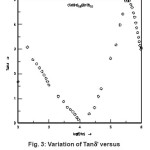
The frequency variation of dielectric loss (tan δ) in each of (CdSe)1-x(ZnS)x samples with x = 0.1 – 1 at room temperature is measured but variations corresponding to the sample with x = 0.2 is shown in Fig. 3.
Figure 1: Variation of ε’ Versus Log of (CdSe)0.8 (ZnS)0.2 Compound with x=0.2
Figure 2: Variation of ε’ versus Log of (CdSe)0.8 (ZnS)0.2 Compound with x=0.2, 0.3 and 1.0
Figure 3: Variation of Tanδ’ Versus Log of (CdSe)0.8 (ZnS)0.2 with x=0.2
Figure 4
It can be seen that tand decreases rapidly with increase in frequency at lower frequencies, dips a minimum at 10 kHz, later it increases with the increase in frequency and reaches a peak at 50 kHz and then decreases similarly all compositions. In all these samples the value of (tan δ) measured at 3000 K decreases from 3.78 to 0.118 when the frequency changed from 100 Hz to 1MHz. The same behaviour was observed in case of AgSbTe2 and in some liquid phases41 From Fig. 3 it is also seen that the dielectric loss (tan δ) dips to a minimum (0.117) at 10 kHz frequency. Further increase in frequency from 10 kHz to 1MHz causes it to increase from 0.117 to 4.92. These changes are almost same for all the samples with x = 0.2 – 1.0. This effect may be due to different sizes of the molecular constituents in the polycrystalline semiconductors in study.
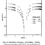
The variation of ac electrical conductivity (σac) with frequency in (CdSe)1-x(ZnS)x samples with x = 0.2, 0.3, 0.5, 0.7 and 1.0 at room temperature is shown in Fig. 4.
The conductivity of all the samples is found to decrease with increase in frequency in the lower frequency region and dip to a minimum at a frequency 10 kHz later, it increases in the higher frequency region, reaches a maximum nearly at 100 kHz and it remains constant beyond 100 kHz. Numerically, at 3000 K the ac conductivity decreases from 79 x 10-4 to 8.9 x 10⁻⁴ mhos in the lower frequency region (100 Hz to 10 kHz) and dips to a minimum at 10kHz and it further increases from 8.9×10⁻⁴ mhos to 87 x 10-4 mhos in the higher frequency region (10 KHz to 1MHz) in sample with x = 0.2. Similarly in sample with x = 0.3, sac decreases from 120 x 10-4 to 14.5 x 10⁻⁴ mhos in the lower frequency region and attains a dip at 10 kHz and further, increases from 14.5 x10⁻⁴ to 118 x 10-4 mhos in the higher frequency region. The obtained minimum and maximum values of sac, in other samples are given in Table 1.
From the Table 1, it may be concluded that the higher and lower values of ac conductivity at lower and higher frequency regions respectively and increase in the value of σac, at 10 kHz with increase in the composition x from 0.2 to 1.0.
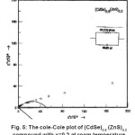
Cole-Cole diagrams for different samples of (CdSe)1-x(ZnS)x are shown in Fig. 5 and the values of ∈s, ∈∞, α, τ0 and τ at room temperature are calculated using these.
These values are consolidated in Table 2. The data from the Table 2 reveals that the molecular relaxation time is less at the end compounds and almost remains constant in the mid compounds. While the static dielectric constant increases from 44.5×10⁶ (for x = 0.2) to 57.93 x 10⁶ (for x = 0.3) and remains almost constant till x = 0.8 and then increases to 90 x 106 as x equals to 1.0.
Figure 5: The cole-Cole Plot of (CdSe)0.8 (ZnS)0.2 Compound with x=0.2 at Room Temperature
Discussion
The dielectric constant of polycrystalline (CdSe)1-x(ZnS)x samples with x = 0.2, 0.3, 0.5, 0.7, 0.8 and 1 over 100 Hz to 1MHz measured at room temperature is higher at low frequencies (Fig. 1). According to Samara,42 the higher the dielectric constant of an ionic crystal, the lower is the energy of formation of lattice defects. Since the grain boundaries of polycrystalline semiconductor contain a large density of defects and according to Halperin43 an ionic component exists reasonably in compound and mixed semiconductors it can be argued that the dielectric constant of (CdSe)1-x(ZnS)x polycrystalline semiconductors should have higher values.
A doped polycrystalline material invariably consists grain or interphase boundaries. These boundaries contain defects such as dangling bonds, vacancies, vacancy cluster etc.44 These defects can cause a positive or negative space charge distribution in interfaces. The space charges can move under the application of an external field and when they are trapped by the defects, many dipole moments are formed (Space charge polarization). Hence the space charge effects the properties inmaterials.45 In addition, ion jump polarization may also be greater in nanocrystalline material since there will be number of positions for the ions to occupy the grain boundaries. The high values of the dielectric constant in the present samples may be attributed to the increased ion jump orientation effect and the increased space charge effect exhibited by polycrystalline particles. Along with these, the dc conductivity effects can also enhance the value of the dielectric constant.46 The large dc conductivity observed in fast ion conductors is interpreted in terms of random hopping of mobile ions from site to site.47 In (CdSe)1-x(ZnS)x material, the presence of high density of trap sites may enhance hopping and thereby an increase in ac conductivity is expected. Also, at low frequencies, the dielectric loss is inversely proportional to frequency, which indicates large dc conductivity,48 and hence an increase in the value of dielectric constant. At high frequencies, as frequency increases a point will be reached where the space charge cannot sustain with the field and hence the polarization decreases, which results in the decrease of ∈’.
The observed variation of dielectric constant ∈’ of the semiconductor with frequency is similar to that of base Ag2HgI4. The addition of alumina nanoparticles enhanced the value of dielectric constant of nano-Ag2HgI4 and the enhancement was found to be a function of the concentration of nano alumina. The insolubility of Al2O3 in Ag2HgI4 as evidenced by X-ray diffraction studies showed that the dispersion alumina nanoparticles of Ag2HgI4 influenced the polarization processes and caused an increase in Î’. Here in the present results dielectric loss and an increase in Î’ in polycrystalline (CdSe)!-x(ZnS)x samples at room temperature has been reported over the frequency range of 100Hz to 1MHz. The polarization in a dielectric material may be contributed by electronic, ionic, dipolar and space charge polarization. All the samples may be active at low frequency.49 The decrease in capacitance with increase in frequency also seems to show the decrease in the number of charge carriers and delay in setting up of dipoles due to availability of very short time in one half cycle of alternating voltages.50 Decrease in the number of charge carriers corresponds to decrease in the polarization.
Figure 5 shows the typical behaviour in the observed capacitance, measured as a function of frequency at different compositions. At room temperature, the capacitance remains constant in the frequency range 100 kHz – 1MHz for various concentrations. For all the samples the capacitance and dielectric constant are observed to reach saturation at high frequencies.
In the present study, tan d is found, initially, to decrease rapidly with increase in the frequency in the lower frequency region and then to increase. We notice a considerable increase of tan δ with frequencies (around 100 kHz) such a behaviour can only be attributed to space charge polarization and relaxation behaviour.58 In nanophase materials, inhomogenities like defects, space charge formation etc., in the interface layers together produce an absorption current resulting in a dielectric loss. Also, enhancement in ac conductivity will give rise to currents which in an ac field are in phase with applied voltage and hence cause dielectric loss.51
The ac conductivity (σac) in all the samples is found to dependent on frequency of the applied field. The conductivity was found initially to decrease with frequency then increase in all samples and increases appreciably with increase in composition from x = 0.2 –1.0. It has been reported that a dispersion in the conductivity is a direct evidence for the hopping of charge carriers around lattice imperfections.52 Dispersion in conductivity will occur when the carriers are not free to move throughout the samples.
According to Sayer and Mansingh53 the frequency dependence of conductivity above 1kHz can be represented by the relation σ(ω) = Aωs, where s is close to unity and the parameter A shows little dependence on temperature. The value of s is the slope of the curve drawn between log σac versus log ω, where w is the angular frequency. The strong dependence of σac on frequency in the high frequency range is typical of highly correlated ionic motion in structurally disordered solid electrolytes.54
It is important to note that the value of s becomes greater than unity was reported for borate glasses by Cramer and Funke55 and was explained on the basis of an additional localized re-orientational ionic motion.
The conductivity enhancement observed in the present investigation can be explained on the basis of the space charge model reported by Maier et al..56 In thermal equilibrium, the surface and grain boundaries of an ionic crystal may carry an electric charge resulting from the presence of excess ions of one sign. This charge is just compensated by a space charge cloud of the opposite sign adjacent to the boundary. For a pure material, the charge arises if the energies to form anion and cation vacancies or interstitials at the boundary are different. The magnitude and sign of the boundary charges change if there are aliovalent solutes present in the matrix, which alter the concentration of the lattice defects in the crystal. Space charge effects will be predominantly important in very small crystals since the grain
boundaries contain a large number of defects compared to the coarser grained poly crystalline materials. The calculated values of DF at different concentrations are shown in Table – 2. Free energy of activation is almost same for all samples. The variation in all the parameters shown in Table – 2 is not appreciable because the Cole-Cole plots are drawn only at room temperature. This reflects on the experimental limitations of not conducting the studies at different temperatures. However, the variation of dielectric constant with frequency helped in modeling the Cole-Cole plots with series resistance and capacitance which are shown in Table – 3 for all samples.
Conclusion
The dielectric properties of (CdSe)1-x(ZnS)x semiconductor compounds with x = 0.2 to 1.0 were investigated in a wide range of frequency from 100Hz to 1MHz at room temperature. ∈’ , tan δ, and σac were found to be larger. The dielectric constant (∈’), at a given frequency, increases with the composition but the nature of decrease in dielectric constant with frequency is almost same in (CdSe)1-x(ZnS)x compounds till the intermediate range of composition but when the composition comes to an end i.e., when x = 1.0 the behaviour differs slightly
The frequency variation of tan δ in (CdSe)1- x(ZnS)x samples with x = 0.2 to 1.0, measured at room temperature, has indicated that tan d decreases rapidly with increase in frequency and dips to a minimum in the lower frequency region and with further increase in frequency, tan δ increases in the higher frequency region.
The ac electrical conductivity (δac) of (CdSe)1- x(Zns)x samples with (x = 0.2 to 1.0) is determined at room temperature is found to decrease in the lower frequency region and dips to a minimum and increases in the higher frequency region. σac also increase largely with the composition.
The variations of ∈’ and a.c conductivity with frequency are explained due to the increased space charge effect at grain boundaries in polycrystalline (CdSe)1- x(ZnS)x mixed semiconductors.
The distribution parameter (α), molecular relaxation time (τ) of (CdSe)1-x(Zns)x semiconductors were calculated from Cole- Cole graphs. The free energy of activation (ΔF) calculated by using molecular relaxation time in the chemical rate theory and found that it is almost same for all (CdSe)1-x(Zns)x samples with x = 0.2 to 1.0.
References
- J.S. Wrran, Nguyen Du., R. Phillippe, G. Stremsdoerfers, Thin Solid Films 144: 117 (1986).
CrossRef
- A.K. Jonscher, M.H. Natho, Thin Solid Films 12: 115 (1975).
- A.M. Abo El Ata, S.M. Attia, T.M. Meaz. Solid State Sciences 6: 61 (2004).
CrossRef
- S.R. Elliott Philos Mag. 36: 1291 (1977).
CrossRef
- N.A. Hegab Ind. J. Pure and Appl. Phys. 39: 586 (2001).
- Mostafa M. Abd El. Raheem, Ind J. Pure and Appl. Phys. 35: 640 (1997).
- S.N. Elsayed and N.H. Mousa, Indian. J. of Pure and Appl. Phys. 33: 185 (1995).
- Sadhana Devi and S.G. Prakash, Indian J. of Pure and Appl. Phys. 30: 75 (1992).
- Sadhana Devi and S.G. Prakash, Indian. J. of Pure and Appl. Phys. 28: 504 (1990).
- P.K.C Pillai, R.Nath and R.C. Ahuja Indian J. Pure & Appl. Phys. 14: 826 (1976).
- A.A. Belov & V.V, Potenkin Radio Ele. & Comm. Syst. (USA), 27: 103 (1984).
- A.M., Bottrean, G Vicq. and A Balana (Ecole Nat Superieure et. in French), J. Mol Liq (Netherlands), 33: 311 (1987).
- K Matsumoto. T Hiuge. & K.Takada ISAF 1986 Proceedings of the 6th IEEE International Symposium on the application of Ferroelectrics (Cat No. 86 CH 2358-0) P.A. Bethlehem, USA, 8, 118 1986 (New York USA, IEEE 1986).
- P Piryatinskii Yu & B.A. Chayanov, Sov. Phys Solid State (USA), 27: 515 (1985).
- V.K. Farkya V.K & N. L. Porwal Indian J. Pure and Appl. Phys. 22: 705 (1984).
- C. Koops, Phys. Rev. 83: 121 (1951).
CrossRef
- A. Dias, R. Luiz Moreire, J. Mater. Res. 12: 2190 (1998).
CrossRef
- D. Diger and K. Ulutas, Vacuum 72: 307 (2004).
CrossRef
- R. N. Dubey and M.S. Qureshi, Ind. J. Pure and Appl. Phys. 41: 40 (2003).
- N.K. Singh and M.K. Choudhary Ind. J of Pure Appl. Phy. 35: 73 (1997).
- S.K. Ubale and C.S. Adgaonkar I JPAP, 39, (2001).
- A.N. Patil, M.G. Patil, K.K. Patnakar, M.L. Mathe, R.P. Mahajan and S.A. Patil, Bull. Mater. Sci. 23: 447 (2000).
CrossRef
- R.P. Mahajan, K.K. Patnakar, N.M. Burange, S.C. Choudhari, Indian J. of Pure and Appl. Phy. 38: 615 (2000).
- M. Chandrashekhar, B. Gopala Krishna, M. Mahesh Kumar and S.V. Suryanarayana, Modern Physics Lett. B, 10: 1365 (1996).
CrossRef
- Ph. Hofmann, K. Horn and A.M. Bradshaw, Physical Review B. 47: 15 (1893).
- Sadao Adachi, J. Appl. Phys. 68: 3 (1999).
- Susumu Ninomiya and Sadao Adachi, J. Appl. Phys. 78: 2 (1995).
- Sadao Adachi, Tushifumi Kumara and Noyishiro Suzuki, J. Appl. Phys. 74: 5 (1993).
CrossRef
- O. Castaing, R. Grauger, J.T. Behhlal and R. Tribourlet. Condens Matter. 8: 5757 (1996).
CrossRef
- L. Benguigui R. Wail, E. Muranerich, A. Chack, and E. Fredy, J. Appl. Phys. 74 (1993).
- T. Gruszecki, B. Holmstrom, Sol. Energy Mater. Sol. Cells 31: 227 (1993).
CrossRef
- S.R. Jawalekar, M.K. Rao, J. Phys. A 54: 223 (1980).
- M.A. El Hiti J. Magretism and Magnetic Materials 164: 187 (1996).
- R.H. Cole and K.S. Cole, J. chem.. phys, 4: 341 (1941).
CrossRef
- H. Fritzsche, In: Amorphous and liquid semiconductors, edited by, J. Tauc (Plenum
Press, New York), 221 (1974).
- M. Cutler, Liquid semiconductors (Academic press, New York) (1977).
- A. Abdelghany, N.. Abdelmohsen, A.H. Abou El Ela and D.M. Abdelwahab, Phys. Chem.
Liq. 19: 33 (1989).
CrossRef
- A. Abdelghany, N. Abdelmohsen, H. H. aboul El Ela and D.A. Abdelwaheb, Ind. J. Pure and
Appl. Phys. 28: 329 (1990).
- J. Maxwell, Electricity and Magnetism, Vol. I Oxford University Press 1873 Section 328.
- K. Wagner, Ann. Phys. 40: 817 (1913).
CrossRef
- S.N. Elsayed, A. Abdelghany, A.H. Abou El Ela and N.H. Mousa Ind. J. Pure and Appl. Phys. 33: 185 (1995).
- G.A.Samara Solid State Phys. 18: 1 (1984).
- W.P. Halperin, Rev. Mod. Phys. 58: 533 (1986).
CrossRef
- Chi-mei Mo, Zhang lide and Wang Gouzhong, Nano-Structured Materials 6: 823 (1995).
CrossRef
- Maier Joachim, Solid State ionic : Materials and Applications (Singapore, World Scientific Publishing Co.) 111, (1992).
- W.D. Kingery, Introduction to ceramics (New York, John Wiley), (1976).
- J.C. Kimball, and Adams Louis, W. Phys. Rev. B. 18: 5851 (1978).
CrossRef
- D.P. Yadav. K.V. Rao. and H.N. Acharya. Phys. Stat. Solidi. A60: 273 (1980).
- S. Mishra, A.V. Krishna Rao and K.V. Rao, Phys. Status Solidi (A), 114: K115 (1989).
CrossRef
- Rodica Turcu, Phys. Status Solidi (A), 119: K121 (1990).
- B.Tareer Phys. of dielectric materials (Moscow. Mir Publishers) (1979).
- D.P Snowden, and H. Saltsburg. Phys. Rev. Lett 14: 497 (1965).
CrossRef
- M. Sayer and Mansingh, Phys. Rev, B 6: 4629 (1972).
CrossRef
- W. Puin and P. Heitjans, Namo structured Materials 6: 885 (1995).
- C. Cramer and K. Funke, Ber. Bunsenges, Phys. Chem.. 96: 1725 (1992).
CrossRef
- Maire Joachim, Solid State Ionic Materials and applications (Singapore World Scientific Publishing Co.) 111 (1992).

This work is licensed under a Creative Commons Attribution 4.0 International License.