Article Publishing History Article Received on : 15 Feb 22 Article Accepted on : 20 Apr 22 Article Published : 25 Apr 2022 Plagiarism Check: Yes Reviewed by: Dr. Mahros Darsin Second Review by: Dr. Kavita singhal Final Approval by: Dr. Prasana Kumar Sahoo
Article Metrics
ABSTRACT:
A high-quality, single-crystal ZnO nanorod thin film was successfully deposited onto p-type monocrystalline silicon (P-Si) substrates using an RF sputtering technique. An XRD analysis of ZnO nanorods was carried out to investigate crystallinity and aspect ratio of the deposited thin film. Adjusting deposition conditions makes it possible to grow single-crystalline ZnO nanorods with preferred orientations (002) on the substrate. More than the substrate type, crystal size is determined by single-crystal growth conditions. These sample had the exact. With the exception of a small variance at Raman shifts 414 cm-1, which correspond to E2. Raman spectra measurements with a slight variation at Raman shifts 414 cm-1, corresponding to E2 (high). In response to the compressive stress, the peak shifts upwards (blue dress). Data from FE-SEM shows vertical growth of hexagonal prism. Finally, the hall effect measurement and UV-vis spectroscopy were carried out the electrical and optical properties of the sample respectively.
KEYWORDS:
Nanorods; R-F sputtering; Raman spectroscopy; Zinc oxide
Copy the following to cite this article:
Aljameel A. I. Single Crystalline Zinc Oxide Nanorods Grown by R-F Sputtering Technique onto P-Si Substrate for Sensing Applications.Mat. Sci. Res. India;19(1).
Copy the following to cite this URL:
Aljameel A. I. Single Crystalline Zinc Oxide Nanorods Grown by R-F Sputtering Technique onto P-Si Substrate for Sensing Applications.Mat. Sci. Res. India;19(1).Available from: https://bit.ly/36RxqNL
Introduction
ZnO is
very low cost and a nontoxic material that can be found naturally as rock salt,
zinc blend and hexagonal structure wurtzite phase1-3. From these
three different phases the wurtzite crystal system is the most common and
famous demonstrated in several activity and stable in a wide range of variation
of surrounding environmental conditions. The lattices constant of this form at
room temperature without strain a=3.25 and c=5.21 in Å unites, with a good
ratio of c/a~1.6, which is perfect matching with the value of the standard
hexagonal structure cell (c/a=1.633)4-5.
ZnO has attracted much attention
due to its optical structural and electrical properties, that make it suitable
for many scientific and industrial applications. ZnO has an exciting
binding energy of 60 mV, which can be consider as partially high value
with a wide direct band gap around 3.37 eV6-8. The unique
properties of ZnO including a photochemical stability, high absorption UV-VIS
region (280-400 nm), strong room temperature luminescence and high
electron mobility are widely applicable in variety potential applications such
as UV photodetectors, sensors and light emitting diodes also it can be
used as antireflection coating, transparent conducting electrode and window
layer to create the np-injunction in solar cell devices. several preparation techniques have been
employed and going on in development as promising methods to synthesis and
fabricate many types and form of ZnO nano structures such as thin films,
nanoparticles, roads, weirs fiber and etc. manly these techniques involve
chemical or physical vapor depositions (CVD or PVD)9-12 and
synthesis in solutions.
The most common techniques are direct
current (DC) and radiofrequency (RF) magnetron-sputtering, thermal evaporation
pulsed laser deposition. Chemical bath deposition, spray pyrolysis,
sol-gel-dip-coating electro-deposition13-15.
Single crystal ZnO nanorods were
fabricated in this work by RF sputtering technique on Si substrates. Optical,
structure and electric properties were discussed.
Materials and Methods
In this work ZnO nanorod arrays have been
deposited onto p-type monocrystalline silicon substrate with orientation of P-Si
(111), and a resistivity value between (1-10 Ω.cm). In the next step we
prepared square 1×1 cm2 P-Si sample. After chemically cleaning via a
standard process the silicon substrates, they were washed in a mixed water-HF (90:10)
solution to reduce the native oxides at surface of Si, which is necessary step before
loaded the sample into a RF magnetron-sputtering system. P-type silicon
substrates were fixed into rotational substrate holder in radio frequency
(RF) magnetron sputtering system. The distance between ZnO target (99.99%
purity) and the substrate was 15 cm and high controllable shutter
properly covered the target. The chamber in the sputtering system was
evacuated to a pressure of 1×10⁻⁷Pa and RF power of 15.80 MHz
applied to produce plasma beam to ejaculate the ZnO target. The ratio of Ar to
O2 controlled via mass flow and gas flowmeter. To avoid
impurities in the deposited thin films, the target was heated and sputtered for
10 minutes. This furthermore fixed the power of produced plasma. RF power
increased to be 280W, and the substrate heated to reach 350 oC. ZnO thin films were sputter
and deposited onto heated and rotted Si substrate for 3min, then the shutter
closed to stop the thin film growth and annealed at 350oC for 30 min. It requires four times of runs
for systems with same process. The total deposition time for four runs was
12 min, while the annealing time was 2 hours in evacuated chamber.
The sputtered ZnO nanorods were examined by employing several procedures through various systems. The thickness of the film has been measured via an optical reflectometer (Filmetric F20). The film structure and crystal quality were studied by a good resolution XRD (PANalytical X’pert PRO MRD PW3040-Netherlands, using a Cu-Kα1 source radiation with wav-length 𝜆 = 1.5406 Å) system, under system resolution of 12 arc/sec. Raman and micro-photoluminescence combined spectrometer model (Jobin Yvon HR800UV) having an argon ion laser (514.5 nm) as a source were used to record the spectrum. FESEM and integrated instrument model: (EDX) (FESEM; Nova Nano SEM 450 – FEI – Japan) is used to analysis the surface morphology and element compositions of sputtered ZnO sample. Finally, the hall effect measurement and UV-vis were carried out the electrical and optical properties of sample respectively.
Results and discussion
XRD analysis
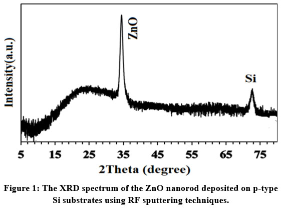
Figure. 1 represents the XRD spectrum of the
ZnO thin film deposited employing the RF sputtering deposition method. The
result indicate that the ZnO thin-film has a single crystal nature with hexagonal
unit cell according to JCPDS card no: 01-076-0704, that has a diffraction peak
at 2θ = 34.798° corresponds to the (002) plane, the obtained
diffraction peak at 2θ =73.78° corresponding to the monocrystalline
Si substrate corresponds to the (100) plane16-17. This refer that
the ZnO monocrystalline film was perpendicular or vertically grown onto the
silicon substrate along the c-axis. The sharp and high peak from
the ZnO film diffraction with small FWHM of 0.34 is strongly confirm that the
deposited is high quality ZnO film.
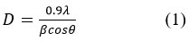
The ordinary crystallite size of ZnO units resembling single peak at (101) is estimated appropriating the Scherer-equation:
the crystallite size is denoted by D
measured in (nm) and 0.9 is called a Scherer constant, while λ is expressed the
wavelength of the X-ray using Cu-Kα source radiation (λ = 0.15406 nm) and theta
measured in degree which is expressed the Bragg angle. β is mean the Full-Width
Half-Maximum (FWHM). The obtained crystallite size was 78 nm.
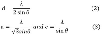
The d-spacing value has been computed from Bragg’s formula (equation (2)), while the lattice constants (a) and (c) were calculated from equations (3).
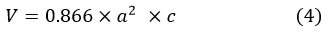
the unit cell volume of ZnO crystal was measured by relation5:
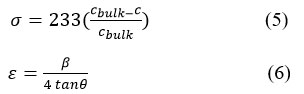
The stress σin GPa unit and the strain along the c-axis plane were measured using equations (5) and (6) respectively12.
the length of chemical bond between Zn and O atoms evaluated via equation 7 and all calculated XRD parameters are listed in table 1.
where
Table 1: The XRD parameters of RF sputtered ZnO thin film.
Parameters
ZnO
2θ (002)
34.798
β
0.1987
D (nm)
79.56
Lattice (a)
3.2333
Lattice (c)
5.2648
a/c
1.6283
d- spacing
2.4656
v
47.41
u
0.4214
L
1.9882
Figure 1: The XRD spectrum of the ZnO nanorod deposited on p-type Si substrates using RF sputtering techniques.
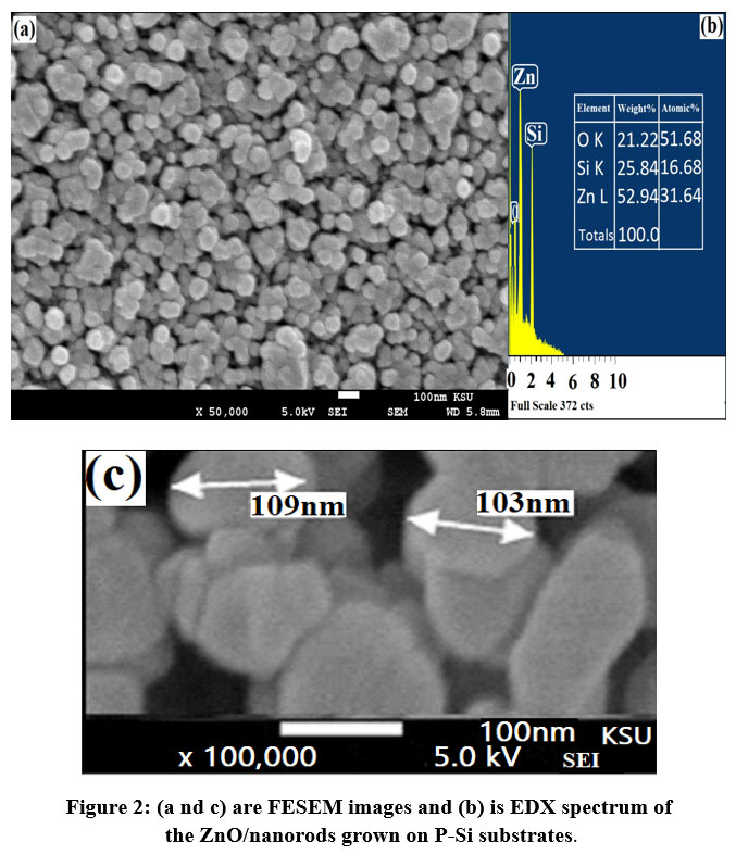
The surface of the ZnO/P-Si was analyzed using FESEM and component elements are analyzed using EDX and their atomic composition is shown in figure 2a. The figure clearly illustrates the smooth, homogeneous, and compact surface of the ZnO nanoparticles without any pores. Shaped ZnO nanorods and the aspect ratio, nanorod lengths, diameters, and nanorod number density correlate with the type of substrate. Based on SEM images, it was found that the diameters of ZnO Nanorods were between 103-109 nm (figure 2c). The percentage gives a description of the atomic composition of the elements in the layers, as shown in the inset table. The peaks show the concentration of these elements, and it is evident that the elements corresponding to the peaks are part of the layer. There were no impurities detected in the samples. This indicts that our sample are with good purity and concentration of ZnO molecules with atoms bonded to Si substrate18-19.
Figure 2: (a nd c) are FESEM images and (b) is EDX spectrum of the ZnO/nanorods grown on P-Si substrates.
The optical characteristics of ZnO/nanorods grown on P-Si
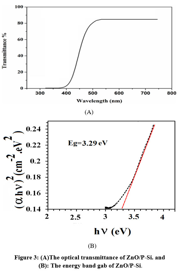
Figure 3(a) displays the transmittance spectrum of gradually annealed and sputtered ZnO films. The film revealed a transmittance of above 85 % in the visible range (300-800 nm)20, which is an excellent optical transmittance. The absorption coefficient (α) calculated from the equation (8) using the optical transmittance spectra.
where ν is the frequency of the photon, (α)
is expressed the absorption-coefficient, (Eg) is the energy gap of
thin film in eV, h is the Planck’s constant, A is a constant, and n associates
with the type of energy band gap due to the electron transition (for directly
band gap n = 1/2).
This method was applied to find the energy ban gap. Consequently, a design of (αE)2 versus photons wave length provided a straight line that cut the wavelength axis at the maximum absorption wavelength at the band gap value as shown in the figure 3(b). The plot of (αE)2 versuswavelengthfor the investigated samples give of energy band gap of 3.29 eV21-22. This fabricated film showed a lessening bandgap that can be attributed to the single and heightened crystallinity.
Figure 3: (A)The optical transmittance of ZnO/P-Si. and (B): The energy band gab of ZnO/P-Si.
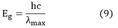
Figure 4 depicts the PL spectrum of ZnO/nanorods on P-Si. A total of 200-1200 nm in wavelength was covered by the spectral data collected. Three peaks may be seen in the results. The highest peak was observed at 377 nm, which corresponded to a monocrystalline ZnO thin film. The greatest values second peak in the green spectrum region are found at wavelengths 548 nm 23. The silicon substrate is responsible for the third peak, which is placed at a wave length of 966 nm. We have maintained that emissions with high green values result from the defect level transition of antisite-oxide atoms (OZn). The oxygen vacancies (VO) and zinc interstitials (Zni) are the primary contributors (donors) to the oxidative stress (Zni). Because of the low production energy of the antisite-oxide, antisite oxide (OZn) in tissues at high oxygen saturation states can be easily formed from interstitial oxides (Oi) and zinc vacancies (VZn) in the presence of oxygen. Several studies have demonstrated that the ionization of individual oxygen-vacancy atoms is effective for the production of green emission, which results from the recombination of photogenerated holes with an individually ionized charge. Equation (8) have been applied to determine the optical energy band-gap (Eg) from the maximum emission wavelength of the ZnO thin film at λmax = 377nm . The obtained result is3.289 eV, which in good agreement with UV result.
Figure 4: PL spectrum of the ZnO nanorods deposited onto P-Si substrates by RF sputtering technique.
Raman spectrum of the sputtered ZnO/nanorods on P-Si
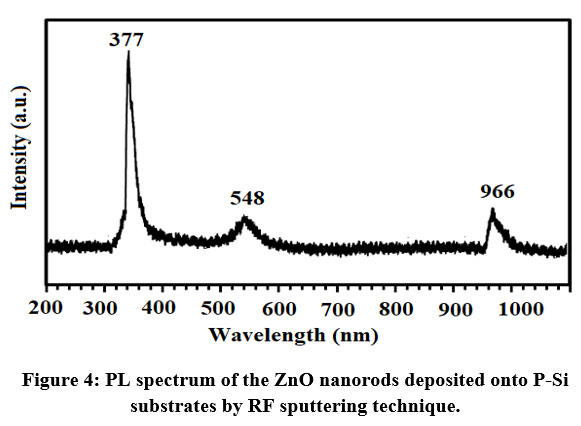
Figure. 5 displays the spectrum of the sputtered ZnO/nanorod layer onto P-Si substrate. Tow Raman shifts at 414 cm-1 and 597 cm-1 were seen for ZnO thin film. The peaks located at 414 cm-1 can be attributed to ZnO E2 (high)while the second on at 597 cm-1 is associated with A1 longitudinal optical (LO) mode. The shift of the E2 (high) from the standard value of the phono mode for the ZnO bulk material 437 cm-1 to was came from the tensile strain in the films, which is highly confirmed the XRD determination. O-vacancy and Zn interstitial are both generate the A1 (LO) phono mode, and the height of the intensity of this mode is direct proportional to these defects in the crystal ZnO thin film. The results also showed that tow Raman shifts at 735 cm-1 and 1077 cm-1 correlated to the P-Si substrate24.
Figure 5: Raman spectrum of the ZnO nanorods grown onto P-Si substrates by RF sputtering technique.
The electrical properties of ZnO/nanorod on P-Si hetero-junction solar cell performance
Measurements
of the electrical properties and performance of a hetero-junction ZnO/nanorods
on P-Si was made utilizing Hall effect
measurement system and by using simulator of solar cell with source light power
of 1000 watts per square meter. The majority of the study is focused on the
development of ZnO/nanorods with high value of transmittance while
simultaneously reducing the values of sheet resistance and resistivity to a
minimum. When measured at 20 degrees Celsius, the resistivity of a hexagonal
wurtzite structures of ZnO is widely known to be in the region of 102 to 104 cm-1.
Because of the electrical properties of ZnO/nanorods, the interstitial atoms of
Zn and the oxygen vacancies dominate the electrons produced by the thin films25-26.
In a laboratory setting, the Van der Pauw method was employed to investigate
the Hall effect27-28. A magnetic field of one tesla (T) was used.
Using aluminum dot electrodes with sizes of a few microns, square shapes were
vaporized (1 x 1 cm2). The impacts of various production processes
on the electric properties of ZnO/nanorods on P-Si are listed in table 2,
starting from sheet resistance and resistivity of sample. The mobility of the
sample and carrier concentration also listed in table 2. On film, the highest
value of 9.85 x 10¹³ N (cm-3) was obtained, showing a
significant drop in carrier concentrations compared to the bulk. The density of
the ZnO thin films appears to be low in SEM images. Because of the tensile
strain, dislocations in the crystal structure and DC-current stress of mobility
deterioration predominate in the sample, resulting in a relatively minor
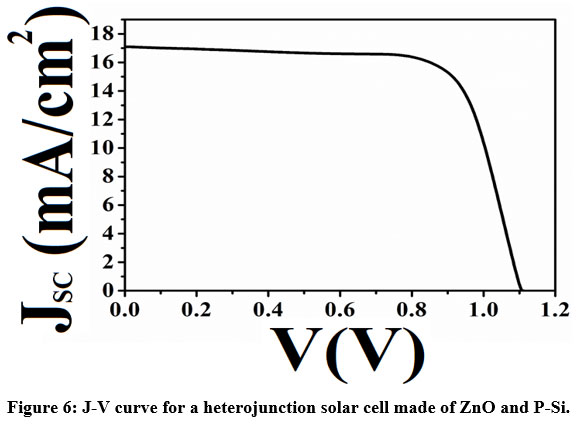
difference in carrier mobility throughout the range of samples. The current-voltage
measurements for an illuminated ZnO/nanorods on P-Si hetero-junction are shown
in figure 6. The PV output parameters are also listed in table 2. This device
had an 11.1 percent efficiency at 1.1 V, a Jsc of 17.1 mA per cm2
and an FF of 73%29. The voltage was just 1.1 V, the current was 17.1
mA per cm2, and the efficiency was 11.1 percent. These acceptable
values are the result of high-quality thin films being used in their
production.
Because of the rise in current density, more ZnO nanoparticles were generated as a result of the bigger grain size than the smaller grain size. Because of the enormous specific surface area of ZnO nanostructures, the efficiency of the solar cell was improved when they were used. Re-crystallizing the films at a higher temperature in order to lower Ohmic contact losses while concurrently increasing recombination losses enhances PV properties while also significantly increasing the performance of the solar cell, according to the researchers.
Figure 6: J-V curve for a heterojunction solar cell made of ZnO and P-Si.
Table 2: The electrical properties and performance of ZnO/P-Si heterojunction solar cell.
Electrical properties
numbers
Sheet resistant (Rs) (Ω /)
8.2 x 10⁴
Resistivity ρ (Ω.cm)
4.2
Carrier concentration N (cm-3)
8.85×10¹³
Hall mobility µH (cm2/V.s)
8.6
J (mA/cm2)
17.1
Voc (V)
1.1
FF (%)
73
Efficiency (η )%
11.2
Conclusions
A study
has been carried out to determine the effect of progressively annealing and
sputtering on the structural, optical, electrical, and mechanical properties of
ZnO/nanorods on a P-Si substrate. The XRD measurements revealed that the ZnO
film was a wurtzite single-crystal structure that grew mostly in the direction
of the c-axis, which was consistent with previous findings. The UV emission
peak that was marked showed a blue shift when compared to the standard baulks
ZnO value. The tensile strain in the films that developed caused a shift in the
Raman phonon modes, which was found to be in excellent agreement with the
results of the XRD investigations. The crown associated with the most
well-known crystal defect (oxygen vacancy) Raman spectra is comparable with the
crown associated with the PL spectrum obtained from the same crystal. The
optical band gap Eg simulated using PL is quite close to the optical band gap
Eg computed from a high transmittance spectrum (above 85 percent) in the
UV-visible region determined using the transmission method.
Acknowledgment
Authors are gratefully acknowledged to the department of Physics and College of Science in Imam Mohammad Ibn Saud Islamic University for their supports in this work.
Conflict of Interest
Author declares that there is no conflict of interest regarding the publication of this article.
Funding Sources
Authors have not received any funding or grant from any institute for the present research.
References
C. Madhumitha, K. Balasubramanian, Enhanced UV photodetection behavior of Cr doped wurtzite ZnO crystalline nanorods, Optical Materials, 110, 110492 (2020). CrossRef
K. Sukriti, P. Chand, Influence of different solvents on the structural, optical, impedance and dielectric properties of ZnO nanoflakes, Chinese journal of physics, 57, 28-46 (2019). CrossRef
Malhotra Satinder Pal Kaur, ZnO nanostructures and nanocomposites as promising photocatalysts for the remediation of wastewater pollution, Environmental Degradation: Causes and Remediation Strategies, Agro Environ Media, Haridwar, India, 120-132(2020). CrossRef
P. Bindu, S. Thomas, Estimation of lattice strain in ZnO nanoparticles: X-ray peak profile analysis, Journal of Theoretical and Applied Physics, 8, 123-134 (2014). CrossRef
A. I. Aljameel, M. K. M. Ali, Zinc oxide thin films preparation by chemical methods onto Si substrate for solar cell application, Journal of Non-Oxide Glasses, 13, 21-29 (2021).
Amaresh Das, Gangadhar Das, Debdulal Kabiraj, Durga Basak, High conductivity along with high visible light transparency in Al implanted sol-gel ZnO thin film with an elevated figure of merit value as a transparent conducting layer, Journal of Alloys and Compounds, 835, 155221 (2020). CrossRef
Serif Ruzgar, Mujdat Caglar, Fabrication and characterization of solution processed Al/Sn: ZnO/p-Si photodiodes, Materials Science in Semiconductor Processing, 115, 105076 (2020). CrossRef
O.F. Farhat, M. M. Halim, M. J. Abdullah, M. K. M. Ali, Naser M. Ahmed, Nageh K. Allam, Growth of vertically aligned ZnO nanorods on Teflon as a novel substrate for low-power flexible light sensors, Applied Physics A, 119, 1197-1201 (2015). CrossRef
Sahar Mohammed Ali, Emad H. Hussein, Osama Abdul Azeez Dakhil, Photocatalytic activity of ZnO/NiO nano-heterojunction synthesized by modified-chemical bath deposition, Nano Futures,5, 035001 (2021). CrossRef
A. Boughelout, R. Macaluso, M. Kechouane, M. Trari, Photocatalysis of rhodamine B and methyl orange degradation under solar light on ZnO and Cu2O thin films, Reaction Kinetics, Mechanisms and Catalysis, 129 1115-1130 (2020). CrossRef
M. Dhanarasu, K. A. Rameshkumar, P. Maadeswaran, Performance, Combustion and Emission evaluation of Direct Injection diesel engine fueled with ZnO dispersed waste cooking oil biodiesel, PREPRINT (Version 1) available at Research Square (2021).
Muhammad Raheel, Different Methods for Detection of Nanoparticles for Semiconductors and Photovoltaic Cells through Diffraction & Novel Approaches, Sch Bull, 7, 264-268 (2021).
Şirin Uzun Çam, Tülay Seri̇n, A. Necmeddin Yazıcı, Effect of Sn doping concentration on structural, optical and electrical properties of ZnS/p-Si (111) diodes fabricated by sol-gel dip-coating method, Materials Science in Semiconductor Processing, 127, 105693 (2021). CrossRef
Dongwan Kim, Jae-Young Leem, Optimal temperature of the sol–gel solution used to fabricate high-quality ZnO thin films via the dip-coating method for highly sensitive UV photodetectors, Journal of the Korean Physical Society, 78, 504-509 (2021). CrossRef
Modou Pilor, Bouchaib Hartiti, Alle Dioum, Hicham Labrim, Youssef Arba, Amine Belafhaili, Mounia Tahri, Salah Fadili, Bassirou Ba, Philippe Thevenin, “The Use of Taguchi Method to Elaborate Good ZnO Thin Films by Sol Gel Associated to Dip Coating, International Journal of Materials Science and Applications, 10, 18(2021). CrossRef
N. Almutlaq, A. F. Al-Hossainy, Novel synthesis, structure characterization, DFT and investigation of the optical properties of diphenylphosphine compound/zinc oxide [DPPB+ ZnO] C nanocomposite thin film, Composite Interfaces, 28, 879-904 (2021). CrossRef
Arafat Toghan, A. Modwi, M. Khairy, Kamal K. Taha, “Influence of TiO2 concentration on the characteristics of ZnO nanoparticles fabricated via sonication assisted with gelatin, Chemical Physics, 551, 111350 (2021). CrossRef
A. Goktas, A. Tumbul, Z. Aba, M. J. T. S. F. Durgun, Mg doping levels and annealing temperature induced structural, optical and electrical properties of highly c-axis oriented ZnO: Mg thin films and Al/ZnO: Mg/p-Si/Al heterojunction diode, Thin Solid Films, 680, 20-30 (2019). CrossRef
S.S. Alias, A. B. Ismail, A. A. Mohamad, Effect of pH on ZnO nanoparticle properties synthesized by sol-gel centrifugation, Journal of Alloys and Compounds, 499, 231-237 (2010). CrossRef
T. Ivanova, A. Harizanova, T. Koutzarova, Bénédicte Vertruyen, Sol-gel derived ZnO: Y nanostructured films: Structural and optical study, Colloids and Surfaces A: Physicochemical and Engineering Aspects, 532, 363-368 (2017). CrossRef
Jeong Chul Lee, Ki Hwan Kang, Seok Ki Kim, Kyung Hoon Yoon, I. Jun Park, Jinsoo Song, RF sputter deposition of the high-quality intrinsic and n-type ZnO window layers for Cu (In, Ga) Se2-based solar cell applications, Solar energy materials and solar cells, 64, 185-195 (2000). CrossRef
A. Modwi, M. K. M. Ali, Kamal K. Taha, M. A. Ibrahem, H. M. El-Khair, M. H. Eisa, M. R. Elamin, O. Aldaghri, Raed Alhathlool, K. H. Ibnaouf, Structural and optical characteristic of chalcone doped ZnO nanoparticles, Journal of Materials Science: Materials in Electronics, 29, 2791-2796 (2018). CrossRef
G.S. Pekar, A. F. Singaеvsky, O. F. Kolomys, V. V. Strelchuk, P. M. Lytvyn, M. M. Osipyonok, I. A. Vasin, M. A. Skoryk, Magnetic and optical properties of printed ZnO: Co polycrystalline layers, Materials Science in Semiconductor Processing,135, 106054 (2021). CrossRef
Fatemeh Abbasi, Fahimeh Zahedi, Mohammad hasan Yousefi, Fabricating and investigating high photoresponse UV photodetector based on Ni-doped ZnO nanostructures, Optics Communications, 482, 126565 (2021). CrossRef
S. Demirezen, H. G. Çetinkaya, M. Kara, F. Yakuphanoğlu, Ş. Altındal. Synthesis, electrical and photo-sensing characteristics of the Al/(PCBM/NiO: ZnO)/p-Si nanocomposite structures, Sensors and Actuators A: Physical, 317, 112449 (2021). CrossRef
S. Tata, L. Chabane, N. Zebbar, M. Trari, M. Kechouane, A. Rahal, Study of morphological and electrical properties of the ZnO/p-Si hetero-junction: Application to sensing efficiency of low concentration of ethanol vapor at room temperature, Materials Science in Semiconductor Processing, 109, 104926 (2020). CrossRef
Christopher J. Perez, Maxwell Wood, Francesco Ricci, Guodong Yu, Trinh Vo, Sabah K. Bux, Geoffroy Hautier, Gian-Marco Rignanese, G. Jeffrey Snyder, Susan M. Kauzlarich, Discovery of multivalley Fermi surface responsible for the high thermoelectric performance in Yb14MnSb11 and Yb14MgSb11, Science advances, 7, 9439 (2021). CrossRef
Chun Li, Lili Zhang, Jiaqi Chen, Xuelian Li, Jingwen Sun, Junwu Zhu, Xin Wang, Yongsheng Fu, “Recent development and applications of electrical conductive MOFs, Nanoscale, 13, 485-509 (2021). CrossRef
M. L. Addonizio, C. Diletto. Doping influence on intrinsic stress and carrier mobility of LP-MOCVD-deposited ZnO: B thin films, Solar Energy Materials and Solar Cells, 92, 1488-149 (2008). CrossRef