M. Kh. Alquran
Department of Applied Science, Ajloun University College, Al-Balqa Applied University Jordan.
Corresponding Author E-mail: mohdquran@bau.edu.jo
DOI : http://dx.doi.org/10.13005/msri/190205
Article Publishing History
Article Received on : 04 May 22
Article Accepted on : 27 May 22
Article Published : 06 Jun 2022
Plagiarism Check: Yes
Reviewed by: Dr. Vinith Bejugam
Second Review by: Dr. Gopalsamy Karuppasamy
Final Approval by: Dr. Sudheesh K. Shukla
Article Metrics
ABSTRACT:
This work aims to assess the enhancement of optical properties for porous GaN nanostructures, which fabricated by Photoelectrochemical etching under different current densities. The changing of optical properties for different samples were investigated by Photoluminescence (PL) spectroscopy. A strong near band-gap-edge emission (NBE) was detected with peak energy 3.40 eV for as-grown and sample etched at 5mA/cm2, while its 3.41 and 3.42 eV for samples etched with 10 and 20mA/cm2 respectively. Also, another peak emission from the sapphire substrate at peak 1.7 eV was observed. The PL peak intensity of the porous samples have increased with increasing the porosity, while the FWHM of the near-band-edge peak was decreased in 5 and 10mA/cm2 samples compared to as-grown non-etched sample, indicated that the pore size decreased with etching current density and porosity. Finally, the change of refractive with porosity was investigated in the porous GaN nanostructure.
KEYWORDS:
Excitation Emission; Photoelectrochemical etching; Porous GaN; Photoluminescence; Porosity; Refractive index
Copy the following to cite this article:
Alquran M. K. Assessment of the Enhancement for the Excitation Emission in Porous GaN Using Photoluminescence. Mat. Sci. Res. India;19(2).
|
Copy the following to cite this URL:
Alquran M. K. Assessment of the Enhancement for the Excitation Emission in Porous GaN Using Photoluminescence. Mat. Sci. Res. India;19(2). Available from: https://bit.ly/3zoPGtZ
|
Introduction
GaN nanostructures have been widely studied, because of their physical and chemical properties compared to those of bulk structure1,2. Small size, band gap shifts and high surface to volume ratio were opened many possibilities for various potential applications in optoelectronics devices. To create GaN nanostructures there are two major methods, bottom up or top down. The bottom up growth methods require sophisticated processes and conditions, such as high temperatures and specific values of pressure. On the oppsite side the top down methods, provide a flexible technique for fabrication GaN nanostructures from normal thin films. Porous semiconductors such as GaN was the famous and simplest example of nanostructures martials fabricated using top down method. In recent years many ways used to fabricate porous GaN using top down method3-10. One of the most top down common and simple techniques to synthesis GaN porous nanostructures is the photo-electrochemical etching (PEC)3-4,11-20. Some advantages of the PEC etching in comparison with other methods are; can be fabricated at room temperature, less damages in the film structurs, simple experiment equpment and process, and low cost. The main parameters in PEC are the voltage, current density, electrolyte composition and illumination21.
Photoluminescence (PL) spectroscopy is one of the highly sensitive techniques used in semiconductors and nanostructures. The quality and the existence of defects in materials can be detected clearly by PL spectroscopy22,23-24. It is a good scientific tool to assess the quality of materials, also many parameters can be calculated from PL spectra.
PL is most techniques used to analyze the optical and electrical properties of porous GaN. The type, energy levels and concentration of point defects in a sample can be calculated from the PL spectra of the samples. PL intensity, energy shift and FWHM of the peaks will give more information about the porous GaN samples and the effect of photoelectrochemical eching on films22. This information will be of great importance to enhance the performance of devices based on GaN material25 and it can be reduced the strain in semiconductor films20.
In this work, we prepared porous GaN nanostructures at room temperature by photo electrochemical etching techniques under different current densities starting from 5 to 20mA/cm2. The optical properties of porous GaN samples were assessment and analyzed deeply using PL spectroscopy.
Experiment Procedure
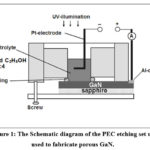
The samples used in this study were commercial n-GaN grown by metalorganic chemical vapor deposition (MOCVD) on the transparents sapphire substrates. Hall measurements confirmed that the electron concentration was n=1 x 1017 cm-3. The samples were cleaned using scientific cleaning processes RCA4,26. To get ohmic contact Aluminum was evaporated under a pressure of 3.4 x 10⁻⁵ Torr on the upper surface of GaN using a thermal evaporation system. Homemade Teflon-cell were used in electrochemical etching process, GaN sample fixed as an anode while the cathode was Pt wire (Figure 1). A mixture of aqueous HF 49% and ethanol C2H5OH 95% 1:4 by volume was an electrolyte. The main variable in the electrochemical etching process was the current density (J), it was changed from 5 to 20 mA/cm2. The etching time is fixed for 20 min and a low power UV lamp (4 W) was used. After the etching, the samples were rinsed in deionized water, and dried in ambient air.
In this work the PL spectroscopy (Jobin Yvon HR800UV system) with high resolution was used to study the optical properties of GaN samples befor and after etching at different current densities. He-Cd laser with an excitation wavelength of 325 nm, with incident laser power 20mW was used, which energy near energy gap of GaN.
Result and Discussion
Figure 2 shows the room temperature PL spectra of Si-doped GaN samples grown on sapphire substrates for as-grown and porous samples etched at different current densities: 5, 10 and 20 mA/cm2. The PL spectrum of porous GaN consists of two major emission peaks: a high intensity peak centerd at UV region, and a weak intensity peak in the visible region. The first peak near band-gap-edge emission (NBE) with peak energy 3.40 eV for as-grown non-etched and sample etched at 5mA/cm2 , while its 3.41 and 3.42 eV for samples etched with 10 and 20 mA/cm2 respectively27. The other peak emission from the sapphire substrate with energy 1.7 eV for all samples28.
 |
Figure 2: PL spectra of porous GaN samples etched under different current densities. Inset shows PL spectra for the range between 1.6 and 1.8 eV.
Click here to View figure
|
For the strong peak there are a small shift to high energy (blue shift) in two samples etched at 10 and 20 mA/cm2 with reletve to as-grown non-etched sample, which indicate a stress increasing in these samples29. The reason of this shift may be due to the development of highly anisotropic structures in the morphology of these samples. This small shift in the strong peak indicating that the pore size has a little effect on the PL peak position. In the other side, the PL peak intensity of the porous samples have increased compared to that of the as-grown one. For samples 5, 10 and 20 mA/cm2, the PL intensity of the first strong beak is enhanced by factors of about 2, 7 and 13 and for the second peak centered at 1.7 eV is enhanced by factors of about 1.5, 6 and 15 (respectively) with compared to the as-grown sample. This increasing of intensities indicating that the number of photons emitted from porous GaN samples is much higher than in the as-grown sample. High surface area and surface roughens in porous samples were increase the reflecting and become the main reason for PL intensity increasing. Yellow, blue and green luminescence were very small peaks or negligible compared to high NBE peak intensity.
The porosity (P) of GaN has one of the main important characteristics, which is defined by this relation30
P = (m1-m2)/(m1-m3) (1)
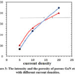
Where m1, m2 and m3 are the mass of the original, anodized, and stripped wafer, respectively. In this work the measured porosities P were 25%, 33%, and 40% of the samples etched with current densities 5, 10 and 20 mA/cm2 respectively.
Figure 3 shows the relation between the current density and porosity, the porosity increased with current densities. Also, the intensity of PL peak increased with increasing in porosity, which indicates that the porosity has a highly influence on the optical properties of porous samples (figure 4A). This increasing could be explained by increasing of light scattering of the new structures of porous samples. In porous samples the surface area per unit volume is very high compare to as grown sample, which provided more exposure of GaN molecules to PL excitation lights and increased the excitation and recombination process of electrons in porous samples.
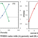
Then the recombination process increased the number of emitted photons in porous samples. Also, porous GaN structures focused the incident light inside the pore nanostructure and increased the light trapping with reduced light losses from surface reflection. The reduction of dislocation density may be contributed in the PL intensity increasing. The shape of PL spectrum depended on the size distribution of nanostructures in porous GaN samples. Many studdieds observed that the increasing of FWHM in photoluminescence is coming from the size of nanostructures such as the pores radius (figure 4A)31. The correlation between the PL spectrum and the pore size is very important issue, which highly effect in devices fabrication depending on porous material.
Since the full-width at half-maximum (FWHM) of PL peaks gives the information about the crystal quality and the size of pores, the FWHM of the PL peaks was measured for porous GaN samples and as-grown. The FWHM of the near-band-edge peak was decreased in 5 and 10mA/cm2 samples compared to as-grown, indicated that the pore size decreased with etching current density and porosity (see figure 4B). While it increased in the 20mA/cm2 may be due to creation of surface disorder and the porosity was very high may be many of the pores being closer together and merge each other, and a blue-shift in emission will occur. The broading in width of the PL peaks, indicated smaller size pores. Among the samples, the change of porosity and the pore size have a little influence on the PL peak shift.
The intensity of the sapphire peak at 1.7 eV was increased with current density and porosity indicated that the etching reached the sapphire substrate and the pore depths was increased with current density and porosity.
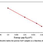
The refractive index (n) of semiconductor material depends on the band gap energy Eg and its decreases with increasing Eg. The velocity of light will be changed when the light move between different materials and then the refractive index will be also changed. There are many approaches to calculate refractive index using the energy gap of semiconductors through simple equations32,33.
In this work the simple Hervé–Vandamme equation was used34:
n2 =1+ [A/(Eg-B) ]2 (2)
Where A and B are constant (A=13.6 eV and B=3.4 eV) for GaN. Figure 5 shows the relation between the refractive index for porous GaN and the energy gap. Therefore, the reflectivity decreased with Eg, this indicated low value of reflectivity and highly interaction with porous GaN samples. Variation in values of (n) is due to successful internal reflections and may be reasoned to photon trapping by grain boundaries35. This may be explaining the high excitation as seen in PL spectra, and this gave a good evidence for the enhancing of optical properties with increasing porosity. The low reflection and high absorption may be attributed to the increase in efficiency of optoelectronic devices.
Conclusions
A simple electrochemical etching method has been applied on GaN to fabricate porous GaN under different current densities. Optical properties of porous GaN were studied using photoluminescence techniques. All samples showed enhancement increasing in PL intensity compared with that of as grown. The values of porosity increased from 25% at current density 5mA/cm2 to 40% at 20mA/cm2. PL intensity, energy gap and FWHM were strong dependence of porosity in all samples. The refractive index of all porous samples was calculated and it was decreased with increasing Eg. The high absorption and low reflection may be attributed to the increase in efficiency of optoelectronic devices. The results in this work indicates that a simple and low-cost electrochemical technique can be used to enhance optical properties of GaN, which can be used to fabricate nanophotonic devices depend on porous GaN with high emission efficiency. These results suggested that photoluminescence is giving a good and a comprehensive technique to investigate the optical properties of nanostructures.
Acknowledgment
Authors are gratefully acknowledged to the department of Applied Science, Al Balqa Applied University, Ajloun College, for their supports in this work.
Conflict of Interest
Author declares that there is no conflict of interest regarding the publication of this article.
Funding Source
Authors have not received any funding or grant from any institute for the present research.
References
- Y. W. Cheng et al., Enhanced light collection of GaN light emitting devices by redirecting the lateral emission using nanorod reflectors, Nanotechnology, 20, 035202 (2009).
CrossRef - J. J. Wierer, A. David, and M. M. Megens, III-nitride photonic-crystal light-emitting diodes with high extraction efficiency, Nat. Photonics, 3, 163 (2009)
CrossRef - K. Al-heuseen, M.R. Hashim, N.K. Ali, Enhanced optical properties of porous GaN by using UV-assisted electrochemical etching, Physica B, 405, 3176 (2010).
CrossRef - K. Al-heuseen, M.R. Hashim, N.K. Ali, Effect of different electrolytes on porous GaN using photo-electrochemical etching, Applied Surface Science, 257, 6197 (2011).
CrossRef - K. Al-heuseen, M.R. Hashim, N.K. Ali, Growth and Characterization of Tree-Like Crystalline Structures during Electrochemical Formation of Porous GaN. Journal of The Electrochemical Society, 158, (5) D240 (2011).
CrossRef - S. Pearton, R.J. Shul, and F. Ren, A Review of Dry Etching of GaN and Related Materials, MRS Internet Journal of Nitride Semiconductor Research, 5, 11 (2000).
CrossRef - H. Hahn, J.B. Gruis, N. Ketteniss, F. Urbain, H. Kalisch, and A. Vescan, Influence of mask material and process parameters on etch angle in a chlorine-based GaN dry etch. J. Vac. Sci. Technol., A 30, 051302 (2012).
CrossRef - Y.F. Zhao, W. Hu, Z. Wei, J.D. Li, S. Yang, Z.L. Huang, Z. Jian, and D.S. An, Controllable process of nanostructured GaN by maskless inductively coupled plasma (ICP) etching, J. Micromech. Microeng, 27, 7 (2017).
CrossRef - Z. Liu, Y.J. Wang, X.X. Xia, H.F. Yang, J.J. Li, and C.Z. Gu, Fabrication of GaN hexagonal cones by inductively coupled plasma reactive ion etching, J. Vac. Sci. Technol., B 34, 4 (2016).
CrossRef - Y. Sun, X. Kang, Y. Zheng, K. Wei, P. Li, W. Wang, X. Liu, and G. Zhang, Optimization of Mesa Etch for a Quasi-Vertical GaN Schottky Barrier Diode (SBD) by Inductively Coupled Plasma (ICP) and Device Characteristics, Nanomaterials, 10, 657 (2020).
CrossRef - M. S. Minsky, M. White, and E. L. Hu, Room‐temperature photoenhanced wet etching of GaN, Appl. Phys. Lett., 68, 1531 (1996)
CrossRef - F. Horikiri, H. Ohta, N. Asai, Y. Narita, T. Yoshida, and T. Mishima, Excellent potential of photo-electrochemical etching for fabricating high-aspect-ratio deep trenches in gallium nitride, Appl. Phys, 11, 091001 (2018).
CrossRef - F. Horikiri, Y. Narita, and T. Yoshida, Excellent wet etching technique using pulsed anodic oxidation for homoepitaxially grown GaN layer, Jpn. J. Appl. Phys, 57, 086502 (2018).
CrossRef - Y. Kumazaki, K. Uemura, T. Sato, and T. Hashizume, Precise thickness control in recess etching of AlGaN/GaN hetero-structure using photocarrier-regulated electrochemical process, J. Appl. Phys, 121, 184501 (2017).
CrossRef - S. G. Lee, S. Mishkat-Ul-Masabih, J. T. Leonard, D. F. Feezell, D. A. Cohen, J. S. Speck, S. Nakanura, and S. P. Den Baars, Smooth and selective photo-electrochemical etching of heavily doped GaN:Si using a mode-locked 355 nm microchip laser, Appl. Phys. Express, 10, 011001 (2017).
CrossRef - C. Youtsey, I. Adesida, and G. Bulman, Highly anisotropic photoenhanced wet etching of 𝑛n-type GaN, Appl. Phys. Lett, 71, 2151 (1997)
CrossRef - L. W. Jang, D. W. Jeon, A. Y. Polyakov, H. S. Cho, J. H. Yun, D. S. Jo, J. W. Ju, J. H. Baek, and I. H. Lee, Free-standing GaN layer by combination of electrochemical and photo-electrochemical etching, Appl. Phys. Express, 6, 061001 (2013)
CrossRef - J. Murata and S. Sadakuni, Electrochim. Photo-electrochemical etching of free-standing GaN wafer surfaces grown by hydride vapor phase epitaxy, Acta, 171, 89 (2015).
CrossRef - C. Zhao, X. Zhang, C.W. Tang, J. Wang, and K.M. Lau, photoelectrochemical wet etching of InGaN nanorods, J.Vac.Sci.Technol, B 38, 060602 (2020).
CrossRef - Y. Alifragis, G. Konstantinidis, A. Georgakilas, N. Chaniotakis, Anion Selective Potentiometric Sensor Based on Gallium Nitride Crystalline Membrane,Electroanalysis, 17, 527 (2005).
CrossRef - L. Lu, Z.Y. Gao, B Shen1, F. J. Xu, S. Huang, Z.L. Miao, Y. Hao, Z.J. Yang, G.Y. Zhang, X.P. Zhang, J. Xu, and D.P. Yu, Microstructure and origin of dislocation etch pits in GaN epilayers grown by metal organic chemical vapor deposition, J. Appl. Phys, 104, 123525 (2008).
CrossRef - T.H. Ngo, B. Gil, T.V. Shubina, B. Damilano, S. Vezian, P. Valvin, and J. Massies, Enhanced excitonic emission efficiency in porous GaN, Sci Rep, 8, 15767 (2018).
CrossRef - S.N. Timoshnev, A.M. Mizerov, G.V. Benemanskaya, et al., Photoemission Studies of the Electronic Structure of GaN Grown by Plasma Assisted Molecular Beam Epitaxy, Phys. Solid State, 61, 2282–2285 (2019).
CrossRef - V. V. Krivolapchuk, M. M. Mezdrogina, A. V. Nasonov, and S. N. Rodin, Photoluminescence of bulk Eu-doped GaN crystals, Physics of the Solid State, 45,1634 (2003).
CrossRef - S.S. Kurbanov, Kh.T. Igamberdiev, T.W. Kang, The UV‐laser induced heating effect on photoluminescence from ZnO nanocrystals deposited on different substrates, J. Phys. D: Appl. Phys, 43, 115401 (2010).
CrossRef - W. Kern, and D.A. Puotien, Cleaning Solutions Based on Hydrogen Peroxide for Use in Silicon Semiconductor Technology, RCA Review, 31, 187 (1970).
CrossRef - H. P. Ho, K. C. Lo, K. Y. Fu, P. K. Chu, K. F. Li, and K. W. Cheah, Synthesis of beta gallium oxide nano-ribbons from gallium arsenide by plasma immersion ion implantation and rapid thermal annealing, Chem. Phys. Lett, 382, 573 (2003).
CrossRef - E. Reuter, R. Zhang, T.F. Kuech, and S. Bishop, Photoluminescence Excitation Spectroscopy of Carbon-Doped Gallium Nitride, MRS Internet Journal of Nitride Semiconductor, 4, 363 (1999).
CrossRef - L.S. Chuah, Z. Hassan, H. Abu hassan, Optical characterization of nanoporous GaN through electroless wet chemical etching, Mater. Sci. Poland, 26, 3 (2008).
- C. Vinegoni, M. Cazzanelli, and L. Pavesi, Silicon-based materials and devices, in: H.S. Nalwa (Ed.), Properties and Devices, vol. 2, (Academic Press, 2001), p. 123.
CrossRef - P. Kumar, Effect of Silicon Crystal Size on Photoluminescence Appearance in Porous Silicon, International Scholarly Research Notices, 2011, 163168 (2011).
CrossRef - Y. Al-Douri, Y. P. Feng, and A. C. H. Huan, Optical investigations using ultra-soft pseudopotential of Si0.5 Ge0.5, Solid State Commun., 148, 521 (2008).
CrossRef - Y. Al-Douri, A. H. Reshak, H. Baaziz, Z. Charifi, R. Khenata, S. Ahmad, U. Hashim, An ab initio study of the electronic structure and optical properties of CdS1− xTex alloys, Solar Energy, 84, 1979 (2010).
CrossRef - P.J.L. Herve, L.K.J. Vandamme, Empirical temperature dependence of the refractive index of semiconductors, J. Appl. Phys., 77, 5476 (1995).
CrossRef - M.J.I. Khan, J. Liu, Z. Kanwal, M.I. Khan, M.N. Usmani, and A.R. Khalid, Investigating optical properties of Cr:GaN system for various Cr concentrations, Mater. Res. Express, 7, 055904 (2020).
CrossRef

This work is licensed under a Creative Commons Attribution 4.0 International License.