Naman Shukla1,3 , Anil Kumar Verma2*and Sanjay Tiwari1
1S.O.S in Electronics and Photonics, Pt. Ravishankar Shukla University, Raipur, Chhattisgarh, India
2Department of Physics, Faculty of Science and Technology, The ICFAI University, Raipur, Chhattisgarh, India.
3Pandit S.N. Shukla University, Shahdol, Madhya Pradesh, India.
Corresponding Author E-mail: anilverma@iuraipur.edu.in
DOI : http://dx.doi.org/10.13005/msri/200104
Article Publishing History
Article Received on : 21 Dec 2022
Article Accepted on : 17 Jan 2023
Article Published : 07 Feb 2023
Plagiarism Check: Yes
Reviewed by: Dr. Pravin Kumar Singh
Second Review by: Dr. Yogesh Chaudhari
Final Approval by: Dr. Saleheh Abbaspoor
Article Metrics
ABSTRACT:
Perovskite-silicon tandem solar cells have attracted much attention to photovoltaic community because of their high efficiency via easy fabrication methods and availability of precursor material abundant in nature. The properties of both perovskite and silicon meet ideal solar cell standards such as high light absorption potential, long carrier diffusion length and fast charge separation process. Semi-transparent solar cell with widely tunable band gap of perovskite material is compatible with silicon solar cell for tandem structures. A perovskite-silicon tandem solar cell four terminal configuration optimization was performed through numerical simulation. The optimized four terminal perovskite-silicon tandem solar cell performances was investigated by varying the thickness of top and bottom solar cell absorber layers, defect density of the absorber layer, and temperature. Perovskite-silicon tandem solar cell showed better photovoltaic performance under constant illumination condition. A high performance mechanically attached four terminal (4-T) perovskite-silicon tandem solar cell has total power conversion efficiency (PCE) of 34.88% by optimized parameters through simulation. It has shown 37% efficiency with matched current of 23.71mA/cm
2. These numerical simulation results are provided the parameter values for further experimental assignment.
KEYWORDS:
Band Gap; Perovskite; Power Conversion Efficiency (PCE); Silicon; Tandem Solar Cell
Copy the following to cite this article:
Shukla N, Verma A. K, Tiwari S. Optimization of Efficient Perovskite-Si Hybrid Tandem Solar Cells. Mat. Sci. Res. India; 20(1).
|
Copy the following to cite this URL:
Shukla N, Verma A. K, Tiwari S. Optimization of Efficient Perovskite-Si Hybrid Tandem Solar Cells. Mat. Sci. Res. India; 20(1). Available from: https://bit.ly/3jBQ16V
|
Introduction
The green and clean solar power resources are achieving the world-wide energy needs, also it reduces the environmental issues like emission of various harmful pollutants which including Carbon-di-Oxide, Carbon Monoxide and Greenhouse gases1. The demand of energy in world could be increased around 30% by the year 2040 2, 3. Fossil fuels are frequently used over the years to satisfy the energy needs. These conventional energy sources are limited in the earth but their combustion causes emission of harmful air pollutants like greenhouse gases, carbon dioxide and carbon monoxide which creates serious concern for global-warming. Solar energy sources became an appropriate and impressive option for reducing carbon footprints and for seamless supply of energy needs in every area such as domestic purpose as well as industrial. The commercial photovoltaic market is mostly based on crystalline silicon (c-Si) solar cell technology 4. Silicon solar cells are used almost everywhere due to its abundant availability in nature, excellent stability and non-toxic properties. The main reason for this is high efficiency and matured technology of converting light energy into electrical energy as well as being of good quality. The PCE of c-Si and thin film technologies of CdTe, CIGS have saturated at ~26% and 23%, respectively within the past decade 5-8. Single junction silicon photovoltaic cell can produce an ideally maximum of PCE up to 31–33% theoretically derived by fundamental Shockley–Queisser (SQ) limit 9. Even after two decades, the efficiency of the single junction silicon photovoltaic technology is stuck at a maximum of about 26% practically due to auger and defect recombination. Perovskite-Si tandem solar cells are alternative to achieve high efficiency above the S-Q limits. Perovskite solar device is made from low cost and simple manufacturing process, possess inherent characteristics like light in weight, flexible, semi-transparent. High efficiency is recently reported by using organic-inorganic lead halide perovskite. It contains tremendous properties such as high absorption coefficient (approximately 105 cm-1) 10, 11 large diffusion length 12, and longer transport distance of electrons and holes. Generally, the organic–inorganic hybrid perovskite has molecular formula ABX3, where A represents MA+ or FA+ (organic cation), B denotes metal cation (Sn2+ or Pb2+, etc.) and X represents halogen anion (F–, Cl–, Br– or I– etc.) 13-15. In perovskite materials, the thermal instability and moisture sensitivity are still under-performed in comparison to silicon materials. CH3NH3PbI3 Perovskite solar cell can get much higher Voc than c-Si and CIGS cells, making them suitable to be the top cells with c-Si bottom solar cell in a tandem structure. They have a tunable band gap, deposited at inexpensive precursors with simple fabrication process, abundant availability in nature, roll-to-roll printing ability, making them ideal candidate materials for tandem solar cells 16-18. Multi-junction solar cells, comprising multiple absorber layers with complementary band gaps, offer a proven approach to reach significantly higher performances. A single solar cell has limitation with parameter of Voc due to relation Eg / q ( Eg is band gap of the active material and q is elementary charge). Due to this, the absorber with narrower band gap can’t produce high Voc. On the other hand, wider band gap absorber is capable to produce high Voc, but the short circuit current (Jsc) is limited. The photons with energy lower than that of the absorber’s band gap, do not participate in photocurrent. Tandem solar cell provides a high Voc and sufficient photocurrent, which is a solution for limitation in single junction solar cell. It contains wide band gap solar cell as well as narrow band gap solar cell in series. The tandem cell absorbs a broad solar spectrum and provides a high Voc, which is the sum of the sub-cell Voc. ‘The generated photocurrent should be balanced because the photocurrent exported from the tandem cell is limited by the sub-cell with the smaller photocurrent.
First time in 2015, perovskite/silicon tandems were realized; the recorded perovskite/silicon device efficiency ranges were below 15%. The journey started with low value of PCEs as comparison to the reported efficiency of the single junction silicon solar cell. Currently, the certified PCEs are reported 29.2% in perovskite/silicon tandem solar cell 5. In the tandem solar device, the perovskite active absorber layer is placed at the top and the silicon at the bottom, with band gaps of 1.54 eV, 1.12 eV respectively. This research paper investigates the unique potential of perovskite/silicon tandem solar cells to achieve a much more efficient conversion of solar energy to electricity. The numerical simulation of perovskite/silicon tandem solar cells was performed. Solar cell capacitance simulator-one dimensional (SCAPS-1D) is utilized intensively for investigating thin film and planar solar cells to examine the outcome of device design, material selection and parameters on their optimum photovoltaic performance. The effect of defect density of the absorber layer, thickness variation of the absorber layer and the temperature variation of perovskite and silicon was studied.
Material and Method
The software of SCAPS-1D is used to perform the numerical simulation of perovskite-silicon tandem solar cell. It is based on solution of Poisson, Continuity, and Transport equations of the generated carriers mainly 19, 20. Poisson’s equation expression is given below:
Where the electrostatic potential is represented by V(x), elementary charge q, absorber permittivity ε, donor and acceptor densities is indicated by ND+, NA– , respectively, and n(x), p(x) are position-dependent electron and hole concentrations, respectively. The expression of continuity equations are given
Where Jn and Jp are electron and hole current density, respectively. R(x) represents the recombination rates and generation rates represented by G(x). The drift- diffusion equation for carriers are given by
Where μn , μp represents the electrons and holes mobility, respectively and Dn, Dp are the electrons and holes diffusion constant, respectively.
In this tandem solar cell, two solar cells are placed one above to the other i.e. in stack form. High energy band gap solar material is placed above and low band energy gap material below it. When the light passes through the front solar cell i.e. the solar cell placed above, the photons of higher energy are absorbed and the remaining photons of less energy are absorbed in the solar cell placed below i.e. silicon solar cell. In other words, as shown in Figure 2, light travels through the transparent electrode and absorbed by the active layer of the perovskite, then it creates electron and hole charge pairs. In this process, short wavelengths take participation. Due to the low binding energy, electron and holes get collected at the electrodes through the respective charge transport layers. Then, the light is passed towards the bottom solar cell. Since the perovskite in the front solar cell is semi-transparent, light easily travels to the silicon solar cell. The absorption of longer wavelength takes place in this cell. In this way, the energy of broad solar spectrum region is absorbed from the tandem solar cell. Firstly, the top cell simulation was performed with the standard AM 1.5G 1 sun spectrum. In case of the bottom cell, the filtered spectrum from the top cell or front solar cell is used in the simulation. In other words, the filtered spectrum is the part of the incident AM 1.5G spectrum, which are not absorbed by top solar cell. An ITO is used for light coupling in between of top and bottom solar cell. The current matching is also required to realize the characteristic of tandem solar cell of two terminal configurations. A fix or constant current is set by controlling the thickness of absorber materials. Many simulations have performed with different concepts and structures of tandem solar cells using SCAPS-1D 21-24.
Energy level and device structure for simulation
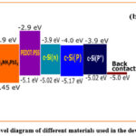 |
Figure 1: (a) Energy Level diagram of different materials used in the device, (b) device structure.
Click here to View Figure
|
Tandem solar cells are mainly fabricated in two terminals and four terminal configurations. In a four-terminal tandem solar cell, there is a mechanical connection between the two sub-solar cells. However, in case of two terminal tandem solar cell configurations, the perovskite solar cells are built on top of silicon based solar cell as shown in Figure 2(a). It means that the sub-solar cells have internal linkage. Currently, certified efficiency reported to be around 29% due to a number of undesirable factors when put into experimental practice 5. The main reasons for the low efficiency are series and parallel resistivity decay, absorption in the inner layers and the effective presence of other environmental conditions. The energy band gap composition in the range of 1.55-1.63 eV is best suitable for front solar cell in tandem structure 25. As shown in Figure 2, light is absorbed from the transparent electrode of a perovskite solar cell (front solar cell) onto the perovskite active layer to form electron-hole pairs. The electron and hole charges get separated due to low binding energy and get collected in the respective electrodes through electron and hole charge transport layer, respectively. In this CH3NH3PbI3 based perovskite solar cell structure, TiO2 is used to facilitate electron charge transport and a thin layer of PEDOT: PSS for hole charge transport in. The optimum performance of the device are set by the varying the thickness of device layer. The thickness of the perovskite active layer in the device is 500 nm, the thicknesses of TiO2 and PEDOT: PSS are 70 nm and 35 nm, respectively. The thickness of the active layer p type doped crystal silicon in the low plane silicon solar cell is 244 micrometers. The thicknesses of c-Si (n) and c-Si back surface field (p+) below are 1.96 µm and 0.03 µm, respectively. Transparent conductive oxides (TCO) thin film is used for light coupling between top cell and bottom cell. Simulation input parameter have been selected from published literature 25-29 and experimental works 30-39. These parameters are listed below in Table 1.
Table 1: Materials input parameters used in the perovskite/silicon solar cell simulation
|
Parameters
|
TiO2
|
CH3NH3PbI3
|
PEDOT:PSS
|
ITO
|
c-Si (n)
|
Si(p+)
|
|
Thickness (µm)
|
0.070
|
0.500
|
0.350
|
0.200
|
1.96
|
0.030
|
|
Band gap, Eg (eV)
|
3.200
|
1.55
|
2.200
|
3.500
|
1.124
|
1.124
|
|
Dielectric permittivity, εr
|
32.00
|
100.00
|
3.000
|
9.00
|
11.9
|
11.9
|
|
Electron affinity, EA (eV)
|
3.9
|
3.900
|
2.900
|
4.00
|
3.9
|
3.9
|
|
CB DOS, Nc (cm−3)
|
1.0E+19
|
2.0E+18
|
2.2E+15
|
2.2E+18
|
2.8E+19
|
2.84E+19
|
|
VB DOS, Nv (cm−3)
|
1.0E+19
|
2.0E+19
|
2.2E+17
|
1.8E+19
|
2.8E+19
|
2.68E+19
|
|
Hole thermal velocity (cm/s)
|
1.0E+7
|
1.0E+7
|
1.0E+7
|
1.0E+7
|
1.0E+7
|
1.0E+7
|
|
Electron thermal velocity (cm/s)
|
1.0E+7
|
1.0E+7
|
1.0E+7
|
1.0E+7
|
1.0E+7
|
1.0E+7
|
|
Electron mobility (cm2/V.s)
|
20
|
1.0
|
2.0
|
20
|
1.25E+3
|
1.212E+3
|
|
Hole mobility (cm2/V.s)
|
10
|
1.0
|
2.0
|
10
|
4.43E+2
|
4.210E+2
|
|
Acceptor concentration (cm−3)
|
0
|
0
|
1.0E+17
|
0
|
0
|
9.5E+20
|
|
Donor concentration (cm−3)
|
1.0E+17
|
1.0E+13
|
0
|
1.0E+18
|
1.0E+17
|
0
|
|
Defect density (cm−3)
|
–
|
1.0E+16
|
–
|
–
|
–
|
–
|
|
Parameters
|
Interfaces
|
|
|
|
|
|
TiO2/ CH3NH3PbI3
|
CH3NH3PbI3/
PEDOT:PSS
|
c-Si(n)/
c-Si (p)
|
c-Si (p)/
c-Si (p+)
|
|
Total defect density (cm-3)
|
1.0×10¹⁵
|
1.0×10¹⁵
|
1.0×10¹⁵
|
1.0×10¹⁵
|
|
Defect type
|
Neutral
|
Neutral
|
Neutral
|
Neutral
|
|
Energetic distribution
|
Gaussian
|
Gaussian
|
Gaussian
|
Gaussian
|
|
Energy level Reference
|
Above VBM
(valence
band maxima)
|
Above VBM
|
Above
VBM
|
Above VBM
|
|
Energy level (eV)
|
0.60
|
0.60
|
0.69
|
0.69
|
|
Capture cross section of electron (cm2)
|
1.0×10⁻¹⁹
|
1.0×10⁻¹⁹
|
1.0×10⁻¹⁹
|
1.0×10⁻¹⁹
|
|
Capture cross section of hole (cm2)
|
1.0×10⁻¹⁸
|
1.0×10⁻¹⁸
|
1.0×10⁻¹⁸
|
1.0×10⁻¹⁸
|
Table 2: 4-T Stacked configuration perovskite-silicon tandem solar cell efficiencies previously reported work.
|
Front solar cell of
perovskite absorber
(band gap)
|
Back solar
cell of Si
|
Voc of
front solar cell, back solar cell
(V)
|
Jsc of front solar cell, back solar cell (mA/cm2)
|
Fill Factor of front solar cell, back solar cell (%)
|
η (%)
|
Author’s Name (Ref.no.)
|
|
FA0.75MA0.15
Cs0.10Rb
(I0.66Br0.33)3 (1.63 eV)
|
Interdigitated back contact Si
|
1.12, 0.73
|
19.4, 18.8
|
0.73, 0.80
|
26.4
|
Duong, T. et al. [33]
|
|
MAPbI3 (1.55 eV)
|
c-Si hetero junction
|
1.07, 0.69
|
20.1, 16.0
|
0.76, 0.80
|
25.2
|
Werner, J. et al. [34]
|
|
MAPbI3 (1.55 eV)
|
Low grade multicrystalline silicon
|
1.03, 0.55
|
17.5, 11.1
|
0.71, 0.70
|
17.0
|
Bailie, C. D. et al. [35]
|
Result and Discussion
The photo-voltaic (PV) characteristics of a perovskite-silicon tandem solar cell were studied through the SCAPS-1D simulation software. The optimized four terminal (4-T) perovskite-silicon tandem solar cell characteristics was observed via thickness variation of top and bottom cell absorber layers, defect density variation of the absorber layer, different concentration of absorber layer, and different temperature level. It is noted from the numerical computation that the tandem solar cell shows better photovoltaic performance under constant illumination condition. A high performance mechanically attached four terminal configuration of perovskite-silicon tandem solar cell showed the efficiency for front and back cell of 25.42% and 20.25%, respectively and overall recorded PCE of 34.88%. The tandem solar cell device and cell structure are depicted in figure 1 (a) and (b), respectively. In perovskite-silicon tandem solar cell structure, c-Si (p+) is used as BSF (back surface field), c-Si (p) is acts as absorber layer and c-Si (n) as the emitter is shown in figure 2. Absorption spectrum of figure 3 confirms better light energy absorption in the solar spectrum region by both the silicon and perovskite materials. It also exhibits the effective absorption capacity of longer wavelengths by silicon. The defect density of active layers of perovskite CH3NH3PbI3 and c-Si (p) was taken as 1.0E+16 and 1.0E+15, respectively. Optimized performance of the multi-junction solar cell was collected at c-Si (p) thickness of 244 µm, c-Si (n) thickness 1.96 µm and perovskite layer 500 nm. The simulation results of front solar cell i.e. perovskite solar cell comprises Voc of 1.26 V, value of Jsc is equal to 23.71 mA/cm2, fill factor 84.78 % and PCE of 25.41%. The simulation of silicon solar cell was performed under filtered spectrum from the top cell. In silicon solar cell, obtained results of the Voc, Jsc, fill factor and PCEs are 0.59 V, 19.34 mA/cm2, 82.76 % and 20.25 %, respectively. In 4-T perovskite-silicon tandem solar cell, the recorded overall efficiency is 34.88%. Thicknesses of absorber layer of front solar cell (Top solar cell) and back solar cell (bottom solar cell) is 500 nm and 264 µm, respectively. A mechanically attached 4-T configuration perovskite-silicon tandem solar cells are optimized, and its performance was studied by varying parameters. The performance of the device is analyzed and also compared with some reported experimental results given in Table 2. The simulated result of 4-T mechanically connected perovskite-silicon tandem device is mentioned in Table 3. It is observed that the perovskite-silicon tandem solar cell raise the performance up to their fundamental SQ limit for single junction solar cells. Energy band diagram (EBG) of perovskite and silicon photovoltaic cell is shown in figure 4. In this EBG, various energy levels i.e. the conduction band energy level (Ec), valence band energy level (Ev) and fermi levels (Fn,Fp) are indicated with respect to layer thickness of the PV cell. Figure 5 represents J-V characteristics of the 4-T perovskite-silicon tandem device. In the J-V characteristics of figure 5 (a), the thickness of silicon (n) is 0.05 µm. In this case, all other parameter is unchanged. The thickness of silicon (n) is optimized to get the best device performance. Now, the optimized thickness of Si (n) is equal to 1.96 µm and corresponding resultant J-V characteristics depicted in figure 5 (b). The increase in current density is indicated on it. The internal quantum efficiency (IQE) of perovskite and silicon PV cell has noticed by figure 6.
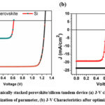 |
Figure 5: 4-T mechanically stacked perovskite/silicon tandem device (a) J-V characteristics before optimization of parameter, (b) J-V Characteristics after optimization
Click here to View Figure
|
Table 3: Photovoltaic parameters in 4-T configuration of perovskite-silicon tandem PV device
|
Solar cell
Parameter
|
Perovskite
|
Silicon
|
Perovskite/silicon tandem
|
|
Voc (Volt)
|
1.26
|
0.59
|
1.26, 0.59
|
|
Jsc (mA/cm2)
|
23.71
|
19.34
|
23.71, 19.34
|
|
FF (%)
|
84.78
|
82.76
|
84.78, 82.76
|
|
η (%)
|
25.41
|
20.25
|
34.88
|
|
V_MPP (Volt)
|
1.12
|
0.51
|
1.12, 0.51
|
|
J_MPP (mA/cm2)
|
22.77
|
18.49
|
22.77, 18.49
|
Absorbing layer of Perovskite and Silicon thickness variation
The thickness of the perovskite layer is one of the effective parameter and has a considerable influence on the characteristics of a solar cell. The simulated results for Voc, FF %, PCE (η) % and Jsc with respect to the variable thickness of perovskite are analyzed, as shown in Figure 7.
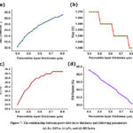 |
Figure 7: The relationship between perovskite layer thickness and following parameters- (a) Jsc (b)Voc (c) η%, and (d) fill factor
Click here to View Figure
|
From figure 7, It is observed that the increase in current density and slightly decrease in Voc as increases in layer thickness of perovskite. Efficiency of the device depends directly on the parameter of Jsc, Voc and fill factor as shown in figure 7 (c). It showed that change in initial value of thickness of perovskite corresponding change in efficiency is high. But, change in thickness of above 600 nm corresponding increase in efficiency is slight.
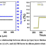 |
Figure 8: The relationship between silicon (p-type) layer thickness and (a) Jsc (b)Voc (c) η%, and (d) Fill factor in silicon photovoltaic device
Click here to View Figure
|
Figure 8 defines the change in parameters by varying the thickness of silicon (p-type) layer. Voc, fill factor and efficiency is constant, not affected by the thickness of silicon (p). However, current density is increased in step manner. Thickness optimization of silicon (n-type) is recorded as shown in figure 9.
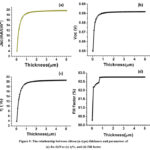 |
Figure 9: The relationship between silicon (n-type) thickness and parameters of (a) Jsc (b)Voc (c) η%, and (d) Fill factor
Click here to View Figure
|
The Voc, Jsc, fill factor and device efficiency increases and saturated after a certain value of thickness of silicon (n). Total recombination and Shockley-Read-Hall (SRH) recombination characteristics of perovskite and silicon are depicted in figure 10(a) and figure 10(b), respectively.
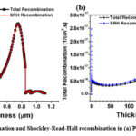 |
Figure 10: Total recombination and Shockley-Read-Hall recombination in (a) Perovskite and (b) Silicon
Click here to View Figure
|
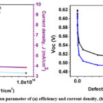 |
Figure 12: Defect density effect on parameter of (a) efficiency and current density, (b) Voc and FF in silicon solar cell
Click here to View Figure
|
Tandem solar cell performances highly are determined by the device configuration and quality of the active layers of perovskite absorber as well as silicon. Absorber layer defect density plays the important role for the optimization of overall device. The film quality is not good in the device, then defect density increases causes decrease in performance and affected all other device characteristics. Poor quality doping process and quality reduction of doping levels of the absorber layers are the leading cause of significant defects and thus low performance device eventually made. The defect density effect on perovskite and solar cell are recorded and as represented in figure 11 and 12, respectively. It has found that the lower defect density in the absorber layer is advantageous for best device performance. Poor quality of absorber layers with high defect densities create a large number of recombination centers and traps, which lead to lower performance. Diffusion length also reduces in case of poor quality of film and thus decreases the lifetime of charge carriers. In this observation of bulk defects for absorber layer determines the carrier lifetime of minority charge carrier, while other interface defects were taken constant. Interface defects usually applied for the determination of recombination velocity at the interface.
The carrier concentration effect on characteristics of perovskite and silicon solar cell are recorded, shown in figure 13 and figure 14, respectively. The dopant carrier concentration is varied from 1.0 x 10¹⁸ to 1.0 x 10¹⁹ to check its influence on solar cell parameters.
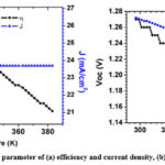 |
Figure 15: Defect density effect on parameter of (a) efficiency and current density, (b) Voc and FF in perovskite solar cell
Click here to View Figure
|
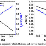 |
Figure 16: Defect density effect on parameter of (a) efficiency and current density, (b) Voc and FF in silicon solar cell
Click here to View Figure
|
Figure 15 and figure 16 represents the effect of temperature on font and back solar cell of tandem structure, respectively. The temperature directly influences the characteristics of the device. Temperature variations were taken within the range i.e. 295 0K to 385 0K for observing characteristics keeping all parameters unaffected. The band gap of absorber layer decreases with an increase in the temperature because lower energy is required for breaking the bond. Thus, open circuit voltage (Voc) and fill factor (FF) decreased in tandem solar cell with the rise in temperature.
Conclusion and future work
A highly efficient perovskite-silicon tandem solar cell was realized using simulation method. Front and back solar cell optimization has been done by setting the optimum value of the parameters such as thickness, carrier concentration, and appropriate value of defect density of the absorber layers. The PV cell based on absorber material of perovskite and silicon has reported efficiency of 34.88 % in 4-T stacked tandem configuration. In this specific structure, the active layer thickness of perovskite and silicon (p) were 500 nm and 244 µm, respectively, which are optimum values for best photovoltaic result. The carrier concentration played the significant role in the device. Therefore, device parameter is observed at different concentration level and selected the best level accordingly, for the best performance. Good morphology of thin films was used for optimum performance. For this purpose, appropriate value for defect density of silicon and perovskite has been taken. The effects of defect density on photovoltaic parameters were studied with respect to absorber layers. The defect density should be as low as it possible, to get a good device performance. Additionally, the device performance was also sensitive to temperature. The device parameters of perovskite silicon tandem were studied by varying the temperature. The absorber perovskite with silicon technology has emerged as a very good technique for increasing the absorption in solar spectrum region. However, many challenges were faced to maintain the crystal structure of perovskite over a larger area as well as the quality of the device must be competing with commercial expectation. It is also necessary to maintain the durability of technology in long-term prospects with respect to stability and sustainability. It is possible to use a 4-T perovskite-silicon tandem photovoltaic cell by separating both the perovskite and silicon solar cells because they’re connected mechanically. Perovskite solar cells work even in the less intense and diffused light received from indoor lighting sources. Therefore, applications are also possible at all other places like indoor windows and walls. Perovskite solar cells are thinner, flexible, and are cost efficient with easy fabrication, creating more opportunities in the field of solar energy.
Acknowledgment
The authors would like to express their sincere thanks to Marc Burgelman and research team for providing the license of SCAPS simulator. One of the authors Dr. Anil Kumar Verma is grateful to Vice Chancellor and Registrar, The ICFAI University, Raipur, Chhattisgarh for their continuous supports.
Conflict of Interest
We declare that there is no conflict of interest regarding the research work carried out for the publication of this article.
Funding Sources
This research work is not sponsored or funded by any institute/organization.
References
- Dresselhause MS, Thomas IL (2001) Alternative energy technologies. Nature 414:332–337.
CrossRef - Jacobson MZ, Delucchi MA, Bauer ZAF, Goodman SC, Chapman WE, Cameron MA, Bozonnat C, Chobadi L, Clonts HA, Enevoldsen P, Erwin JR, Fobi SN, Goldstrom OK, Hennessy EM, Liu J, Lo J, Meyer CB, Morris SB, Moy KR, O’Neill PL, Petkov I, Redfern S, Schucker R, Sontag MA, Wang J, Weiner E, Yachanin AS (2017) 100% clean and renewable wind, water, and sunlight all-sector energy roadmaps for 139 countries of the world, Joule 1, 1–14, Elsevier Inc
CrossRef - EIA (Energy Information Administration, U.S.) (2017) International Energy Outlook 2014 DOE/EIA-0484(2014) (U.S. Department of Energy). https://www.eia.gov/todayinenergy/detail.php?id=32912
- F. I. S. E. Systems. ISE. (2020). Photovoltaics Report. https://www.ise.fraunhofer.de/content/dam/ise/de/documents/publications/studies/Photovoltaics-Report.pdf
- National Renewable Energy Laboratory, Best research-cell efficiencies. https://www.nrel.gov/pv/assets/pdfs/best-research-cell-efficiencies.20200104.pdf
- Tiwari S, Tiwari S (1994) A novel technique for enhancing efficiency and stability of CdTe based PEC solar cells. J Phys D Appl Phys 27:2009–2012.
CrossRef - Mishra S, Tiwari S, Chandra BP (1995) Optimization of photoelectrochemical solar cells based on polycrystalline CdTe film photoanode. Sol Energy Mater Sol Cells 37(2):133–142
CrossRef - Tiwari S, Tiwari S (2006) Development of CdS based stable thin film photo electrochemical solar cells. Sol Energy Mater Sol Cells 90(11):1621–1628.
CrossRef - Shockley, W., Queisser, H. J. (1961). Detailed balance limit of efficiency of p‑n junction solar cells, J. Appl. Phys. 32, 510.
CrossRef - Krishna, B., Rathore, G., Shukla, N. and Tiwari, S. (2021). Perovskite solar cells: A review of architecture, processing methods, and future prospects. Hybrid Perovskite Composite Materials, WoodheadPublishing, Pages 375-412. https://doi.org/10.1016/B978-0-12-819977-0.00018-4.
CrossRef - Green, M., Ho-Baillie, A. and Snaith, H. (2014). The emergence of perovskite solar cells. Nature Photon 8, 506–514.
CrossRef - Stranks, S. D., Eperon, G. E., Grancini, G., Menelaou, C., Alcocer, M. J. P., Leijtens, T., Herz, L. M., Petrozza, A. &Snaith, H. J. (2013). Electron-hole diffusion lengths exceeding 1 micrometer in an organometaltrihalideperovskite absorber. Science 342, 341–344.
CrossRef - Giorgi, G., Fujisawa, J. I., Segawa, H., & Yamashita, K. (2013). Small photocarrier effective masses featuring ambipolar transport in methylammonium lead iodide perovskite: A density functional analysis. The journal of physical chemistry letters, 4 (24), 4213-4216.
CrossRef - Goldschmidt, V. M. (1927). Crystal structure and chemical correlation. Ber. Dtsch. Chem. Ges, 60, 1263-1296.
CrossRef - Rini, M., Dean, N., Itatani, J., Tomioka, Y., Tokura, Y., Schoenlein, R. W., Cavalleri, A. (2007). Control of the electronic phase of a manganite by mode-selective vibrational excitation. Nature, 449(7158), 72-74.
CrossRef - Tan, Z.K., Moghaddam, R.S., Lai, M.L., Docampo, P., Higler, R., Deschler, F., Price, M., Sadhanala, A., Pazos, L.M., Credgington, D., Hanusch, F., Bein, T., Snaith, H.J. and Friend, R.H. (2014). Bright light-emitting diodes based on organometal halide perovskite. Nat Nanotechnol. 9(9):687-92. https://doi.org/10.1038/nnano.2014.149
CrossRef - Eperon,G. E.,Stranks,S. D.,Menelaou, C.,Johnston,M. B., Herz,L. M. and Snaith,H. J. (2014). Formamidinium lead trihalide: a broadly tunable perovskite for efficient planar heterojunction solar cells, Energy Environ. Sci., 7-982–988.
CrossRef - Tiwari S., Tiwari T., Carter S.A., Scott J.C., Yakhmi J.V. (2019) Advances in Polymer-Based Photovoltaic Cells: Review of Pioneering Materials, Design, and Device Physics. In: Martínez L., Kharissova O., Kharisov B. (eds) Handbook of Ecomaterials. Springer, Cham. https://doi.org/10.1007/978-3-319-68255-6_59
CrossRef - Burgelman, M., Decock, K., Khelifi, S. and Abass, A. (2013). Advanced electrical simulation of thin film solar cells. Thin Solid Films. 535, 296-301.
CrossRef - Burgelman, M., Nollet, P. and Degrave, S. (2000). Modelling polycrystalline semiconductor solar cells. Thin Solid Films. 361-362, 527-532.
CrossRef - Madan J, Shivani Pandey R, Sharma R (2020) Device simulation of 17.3% efficient lead-free all-perovskite tandem solar cell. Sol Energy 197:212–221. https://doi.org/10.1016/j.solener.2020.01.006
CrossRef - Kim K, Gwak J, Ahn SK, Eo YJ, Park JH, Cho JS, Kang MG, Song HE, Yun JH (2017) Simulations of chalcopyrite/c-Si tandem cells using SCAPS-1D. Sol Energy 145:52–58. https://doi.org/10.1016/j.solener.2017.01.031
CrossRef - Islam MT, Jani MR, Islam AF, Shorowordi KM, Chowdhury S, Nishat SS, Ahmed S (2021) Investigation of CsSn0.5Ge0.5I3-on-Si tandem solar device utilizing SCAPS simulation. IEEE Trans Electron Devices 68:618–625. https://doi.org/10.1109/TED.2020.3045383
CrossRef - N. Singh, A. Agarwal, M. Agarwal, Numerical Simulation of highly efficient lead-free perovskite layers for the application of all-perovskite multi-junction solar cell, Superlattices and Microstructures, https://doi.org/10.1016/j.spmi.2020.106750.
CrossRef - Leijtens, T., Eperon, G.E., Pathak, S., Abate, A., Lee, M.M. and Snaith, H.J. (2013) Overcoming ultraviolet light instability of sensitized TiO2 with meso-superstructured organometal tri-halide perovskite solar cells, Nat. Commun. 4, 2885.
CrossRef - M. Liu, M. B. Johnston, H. 1. Snaith. Efficient planar heterojunction perovskite solar cells by vapour deposition. Nature, vo1.7467, pp.395-398 (2013).
CrossRef - H. J. Snaith. Perovskites: the emergence of a new era for low cost, high-efficiency solar cells. J. Phys. Chem. Lett. Vol. 4 pp.3623-3630 (2013).
CrossRef - Patel, P.K. (2021). Device simulation of highly efficient eco‑friendly CH3NH3SnI3 perovskite solar cell, Scientific Reports 11:3082.
CrossRef - Shukla, N. et al. (2021). Investigation on Design and Device Modeling of High Performance CH3NH3PbI3-xClx Perovskite Solar Cells. Journal of Ravishankar University (Part-B: Science), 34(1), pp. 58-63. https://doi.org/10.52228/JRUB.2021-34-1-8
CrossRef - Kischkat, J., Peters, S., Gruska, B., Semtsiv, M., Chashnikova, M., Klinkmüller, M., … & Masselink, W. T. (2012). Mid-infrared optical properties of thin films of aluminum oxide, titanium dioxide, silicon dioxide, aluminum nitride, and silicon nitride. Applied optics, 51(28), 6789-6798.
CrossRef - Green, M. A. (2008). Self-consistent optical parameters of intrinsic silicon at 300 K including temperature coefficients. Solar Energy Materials and Solar Cells, 92(11), 1305-1310.
CrossRef - Ball, J. M., Stranks, S. D., Hörantner, M. T., Hüttner, S., Zhang, W., Crossland, E. J., … & Snaith, H. J. (2015). Optical properties and limiting photocurrent of thin-film perovskite solar cells. Energy & Environmental Science, 8(2), 602-609.
CrossRef - Duong, T., Wu, Y., Shen, H., Peng, J., Fu, X., Jacobs, D., … & Catchpole, K. (2017). Rubidium multication perovskite with optimized bandgap for perovskite‐silicon tandem with over 26% efficiency. Advanced Energy Materials, 7(14), 1700228.
CrossRef - Werner, J., Barraud, L., Walter, A., Bräuninger, M., Sahli, F., Sacchetto, D., … & Ballif, C. (2016). Efficient near-infrared-transparent perovskite solar cells enabling direct comparison of 4-terminal and monolithic perovskite/silicon tandem cells. ACS Energy Letters, 1(2), 474-480.
CrossRef - Bailie, C. D., Christoforo, M. G., Mailoa, J. P., Bowring, A. R., Unger, E. L., Nguyen, W. H., … & McGehee, M. D. (2015). Semi-transparent perovskite solar cells for tandems with silicon and CIGS. Energy & Environmental Science, 8(3), 956-963.
CrossRef - Wu, Y. et al. Monolithic perovskite/silicon-homojunction tandem solar cell with over 22% efficiency. Energy Environ. Sci. 10, 2472–2479 (2017).
CrossRef - Werner, J., Weng, C. H., Walter, A., Fesquet, L., Seif, J. P., De Wolf, S., … & Ballif, C. (2016). Efficient monolithic perovskite/silicon tandem solar cell with cell area> 1 cm2. The journal of physical chemistry letters, 7(1), 161-166.
CrossRef - Mailoa, J. P., Bailie, C. D., Johlin, E. C., Hoke, E. T., Akey, A. J., Nguyen, W. H., … & Buonassisi, T. (2015). A 2-terminal perovskite/silicon multijunction solar cell enabled by a silicon tunnel junction. Applied Physics Letters, 106(12), 121105.
CrossRef - Rai, N., Rai, S., Singh, P. K., Lohia, P., & Dwivedi, D. K. (2020). Analysis of various ETL materials for an efficient perovskite solar cell by numerical simulation. Journal of Materials Science: Materials in Electronics, 31(19), 16269-16280.
CrossRef

This work is licensed under a Creative Commons Attribution 4.0 International License.


